Insulated gate bipolar transistor (IGBT) device

A device and trench gate technology, applied in the field of insulated gate bipolar transistor devices, can solve the problems of increasing Miller capacitance Cgc, affecting the stability of device turn-on characteristics, gate overshoot voltage stability, and increasing device turn-off loss. Achieve the effect of reducing on-state voltage drop, improving stability and increasing current density

Active Publication Date: 2018-08-17
SHANGHAI HUAHONG GRACE SEMICON MFG CORP
View PDF5 Cites 2 Cited by
  • Summary
  • Abstract
  • Description
  • Claims
  • Application Information

AI Technical Summary

Problems solved by technology

[0011] 1. Due to the large lateral area of ​​the P-float104a, the Miller capacitance Cgc increases, which affects the turn-on characteristics of the device and the stability of the gate overshoot voltage
[0012] 2. Wh

Method used


Image

  • Insulated gate bipolar transistor (IGBT) device
  • Insulated gate bipolar transistor (IGBT) device
  • Insulated gate bipolar transistor (IGBT) device

Examples


Embodiment I

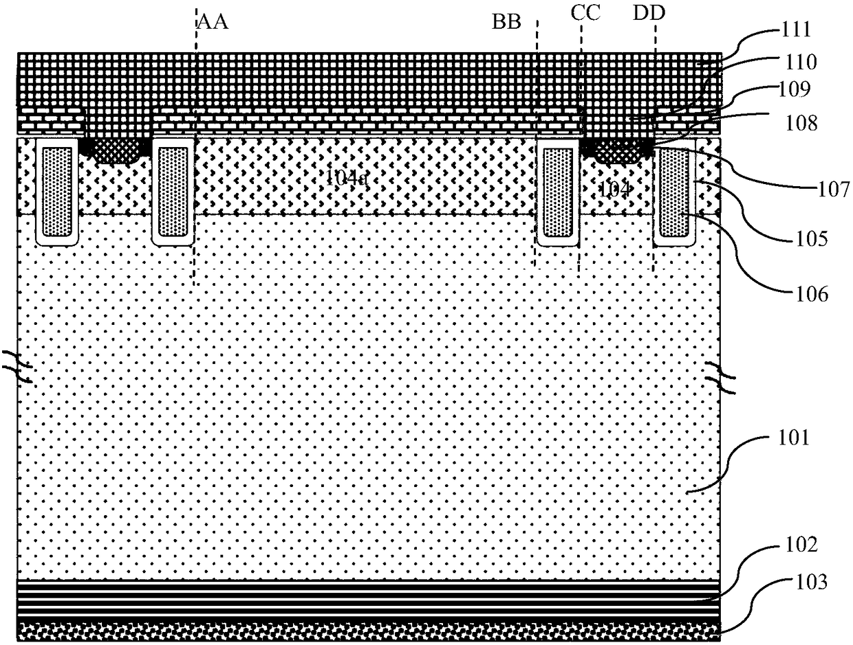
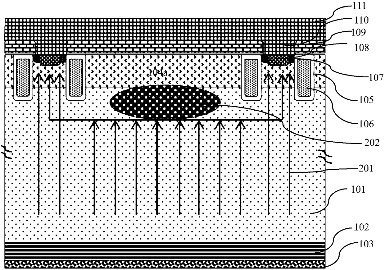
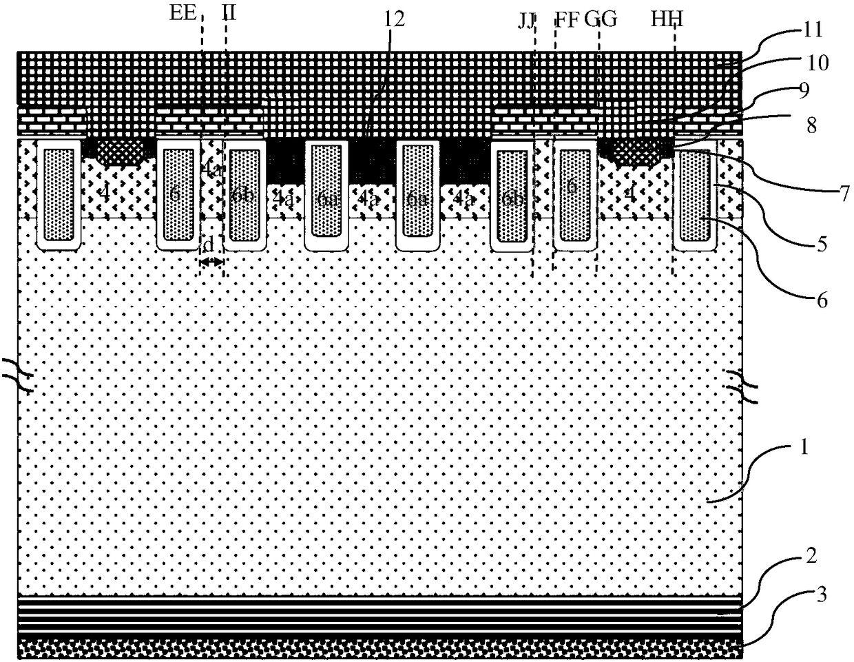
[0045] Such as image 3Shown is a schematic structural diagram of the IGBT device of the embodiment of the present invention. The IGBT device of the embodiment of the present invention includes:

[0046] Drift region 1 of the first conductivity type.

[0047] A collector region 3 with a second conductivity type heavily doped is formed on the back of the drift region 1 .

[0048] Preferably, there is also a buffer layer 2 between the drift region 1 and the collector region 3, and the buffer layer 2 has a doping concentration of the first conductivity type doped with a doping concentration greater than that of the drift region 1. miscellaneous. Here, the buffer layer 2 has the function of accelerating the decrease rate of the electric field intensity in the drift region 1 , so it is also called a field stop layer, ie, an FS layer.

[0049] At least two first trench gates, at least one side surface of each first trench gate is formed with a channel region 4, the channel region...


PUM


Abstract

The invention discloses an insulated gate bipolar transistor (IGBT) device. The IGBT device comprises at least two first groove gates and at least one flotation region, wherein a channel region is formed on at least one side surface of each first groove gate, two sides of the flotation region are limited by side surfaces of the two corresponding first groove gates, at least one second groove gateis formed in the flotation region and penetrates through the floating region, a first well region oppositely doped is formed on a surface of the flotation region, an emission region is formed on a surface of the channel region, a surface of the emission region is connected to an emitter via a contact hole, a surface of the first well region is also connected to the emitter via the contact hole, the second groove gate is connected to a control signal, the channel on the side surface of the second groove gate is switched off by the control signal when the IGBT device is conducted so that carriers are accumulated in the flotation region, and the channel on the side surface of the second groove gate is switched on by the control signal when the IGBT device is switched off so that the accumulated carriers are released. By the IGBT device, the on-state voltage drop of the device can be simultaneously reduced, and the switch-off loss of the device is reduced.

Description

technical field [0001] The present invention relates to a semiconductor integrated circuit, in particular to an insulated gate bipolar transistor (Insulated gate bipolar transistor, IGBT) device. Background technique [0002] The IGBT has both the voltage control of the insulated gate field effect transistor (MOSFET) and the low on-resistance and high withstand voltage characteristics of the bipolar transistor (BJT). , Low switching loss and many other excellent characteristics, are widely used in medium and high power power electronic systems. [0003] Such as figure 1 Shown is a schematic structural diagram of an existing IGBT device. Taking an N-type device as an example, the existing IGBT device includes: [0004] A collector region 103 composed of a P+ region formed on the back of the silicon wafer, an N-type doped buffer layer (Buffer) 102 formed above the collector region 103, a drift region 101 composed of an N-doped region, The doping concentration of the buffer ...

Claims


Application Information

Patent Timeline
IPC IPC(8): H01L29/739H01L29/06H01L29/423
CPCH01L29/0603H01L29/0684H01L29/423H01L29/7397
Inventor 张须坤
Owner SHANGHAI HUAHONG GRACE SEMICON MFG CORP
Why Eureka
Try Eureka