Platinum telluride two-dimensional material as well as preparation thereof and application thereof in electrical devices

A two-dimensional material, platinum telluride technology, applied in the field of nanomaterials, can solve the problem that two-dimensional platinum telluride nanosheets have not been studied, and achieve the effects of good controllability and reproducibility, simple equipment, and improved regularity

Active Publication Date: 2018-08-24
HUNAN UNIV
View PDF3 Cites 11 Cited by
  • Summary
  • Abstract
  • Description
  • Claims
  • Application Information

AI Technical Summary

Problems solved by technology

[0004] Despite such great potential of PtTe, there is no reported method to prepare 2D PtTe nanosheets, including the preparation of 2D PtTe nanosheets with various thicknesses, regular shapes and good crystallinity.

Method used


Image

  • Platinum telluride two-dimensional material as well as preparation thereof and application thereof in electrical devices
  • Platinum telluride two-dimensional material as well as preparation thereof and application thereof in electrical devices
  • Platinum telluride two-dimensional material as well as preparation thereof and application thereof in electrical devices

Examples


Embodiment 1

[0086] Preparation of platinum telluride nanosheets:

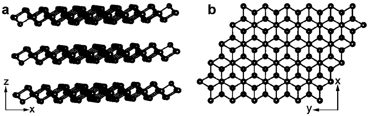
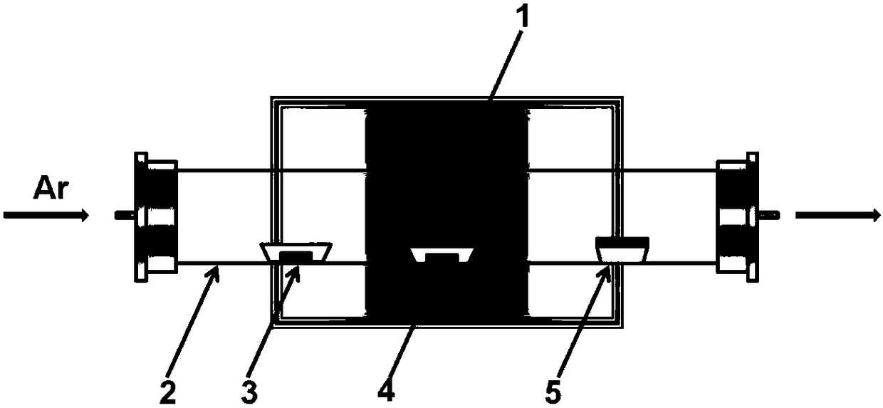
[0087] Put the porcelain boat containing 0.04g platinum powder (particle size ≤ 1μm) in the constant temperature zone of the tube furnace, and the porcelain boat containing 0.6g tellurium powder (particle size 38-74μm) in the upstream of the tube furnace Variable temperature zone, the temperature is 500°C, a piece of 300nm SiO 2 / Si as PtTe 2The bright side of the growth substrate was placed on another porcelain boat and placed in the temperature-changing zone downstream of the furnace to obtain an appropriate crystal growth temperature. Before heating, exhaust the air in the quartz tube with a large flow of argon. Then the furnace is heated up to 1000°C, and the argon gas flow rate is 50 sccm, and the temperature is kept constant for 40 minutes, and single crystal platinum telluride nanosheets will be formed at a position of 720°C in a certain temperature range of the silicon wafer. The experimental setup of platinum t...

Embodiment 2

[0090] Preparation of platinum telluride nanosheets:

[0091] Put the porcelain boat containing 0.04g platinum powder (particle size ≤ 1μm) in the constant temperature zone of the tube furnace, and the porcelain boat containing 0.6g tellurium powder (particle size 38-74μm) in the upstream of the tube furnace The temperature in the variable temperature zone is 500°C, and a piece of 300nm SiO 2 / Si as PtTe 2 The bright side of the growth substrate was placed on another porcelain boat and placed in the variable temperature zone downstream of the furnace to obtain an appropriate crystal growth temperature. Before heating, exhaust the air in the quartz tube with a large flow of argon. Then the furnace is heated up to 1050°C, and the argon flow rate is 80sccm, and the temperature is kept constant for 30 minutes, and single crystal platinum telluride nanosheets will be formed at a position of 700°C in a certain silicon wafer temperature range. The experimental setup of platinum te...

Embodiment 3

[0094] Preparation of platinum telluride nanosheets:

[0095] Put the porcelain boat containing 0.04g platinum powder (particle size ≤ 1μm) in the constant temperature zone of the tube furnace, and the porcelain boat containing 0.6g tellurium powder (particle size 38-74μm) in the upstream of the tube furnace The temperature in the variable temperature zone is 480°C, and a piece of 300nm SiO 2 / Si as PtTe 2 The bright side of the growth substrate was placed on another porcelain boat and placed in the variable temperature zone downstream of the furnace to obtain an appropriate crystal growth temperature. Before heating, exhaust the air in the quartz tube with a large flow of argon. Then the furnace is heated up to 1100°C, and the argon gas flow rate is 120 sccm, and the temperature is kept constant for 25 minutes. At the position of 680°C in a certain silicon wafer temperature range, single crystal platinum telluride nanosheets will be formed. The experimental setup of platin...


PUM

PropertyMeasurementUnit
thicknessaaaaaaaaaa
particle diameteraaaaaaaaaa
sizeaaaaaaaaaa

Abstract

The invention belongs to the field of nano material preparation, and in particular discloses a platinum telluride two-dimensional material, i.e., platinum telluride nanosheets. The invention also provides a preparation method of the platinum telluride two-dimensional material; the method comprises the steps of enabling tellurium powder and platinum powder to be volatilized at a temperature not lower than 410 DEG C and a temperature of 1000-1170 DEG C respectively, and enabling the volatilized tellurium and platinum to be deposited on the surface of a substrate by means of chemical vapor deposition under the conditions that the carrier gas flow is 50-400sccm and the temperature is 350-720 DEG C so as to obtain the platinum telluride nanosheets. The invention also relates to the platinum telluride two-dimensional material prepared by the method, optical devices prepared from the platinum telluride two-dimensional material, and especially comprises application of the platinum telluride two-dimensional material in PtTe2 field effect transistors. The platinum telluride nanosheets are good in morphology and are hexagonal and triangular, have thicknesses of 2-40nm and sizes of 1.5-52mu m,and are good in crystallinity; the preparation method is simple and easy to implement.

Description

technical field [0001] The invention belongs to the field of nanometer materials, in particular to platinum telluride two-dimensional materials, preparation and application in electrical devices. technical background [0002] Since 2004 graphene 1-3 The successful preparation proved that two-dimensional materials can exist stably in nature, and also started a research boom of two-dimensional nanomaterials. Graphene is a two-dimensional material with a single atomic layer. It has attracted great attention of scientists all over the world because of its excellent properties in electricity, mechanics, heat and optics. However, single-layer graphene does not have a band gap, which limits its application in logic circuits. In order to make up for the lack of zero band gap in graphene, scientists began to look for other compounds with similar layered structure characteristics, such as hexagonal boron nitride (h-BN) 4 , transition metal dichalcogenides (TMDs) 5-7 and black phos...

Claims


Application Information

Patent Timeline
Patent Type & Authority Applications(China)
IPC IPC(8): C30B29/46C30B29/64C30B25/00H01L29/24H01L29/78
Inventor 段曦东段镶锋马惠芳
Owner HUNAN UNIV
Why Eureka
Try Eureka