Multiband sample irradiation device based on atomic force microscope

An atomic force microscope and irradiation device technology, applied in the field of electrical, magnetic, material surface morphology and mechanical, thermal performance testing, can solve the problem that the relevant performance cannot be guaranteed to not change again, the analysis accuracy is limited, and the surface performance index cannot be changed. Real-time analysis and other issues to achieve the effect of power density adjustment, power adjustment, and interference avoidance

Active Publication Date: 2018-08-24
BEIHANG UNIV
View PDF13 Cites 1 Cited by
  • Summary
  • Abstract
  • Description
  • Claims
  • Application Information

AI Technical Summary

Problems solved by technology

This type of method cannot perform real-time analysis of the changes in the surface properties of the samples during the irradiation process, and at the same time cannot guarantee that the relevant properties of the irradiated samples will not change during the storage and testing stages, which limits the accuracy of the analysis.

Method used


Image

  • Multiband sample irradiation device based on atomic force microscope
  • Multiband sample irradiation device based on atomic force microscope
  • Multiband sample irradiation device based on atomic force microscope

Examples


Embodiment 1

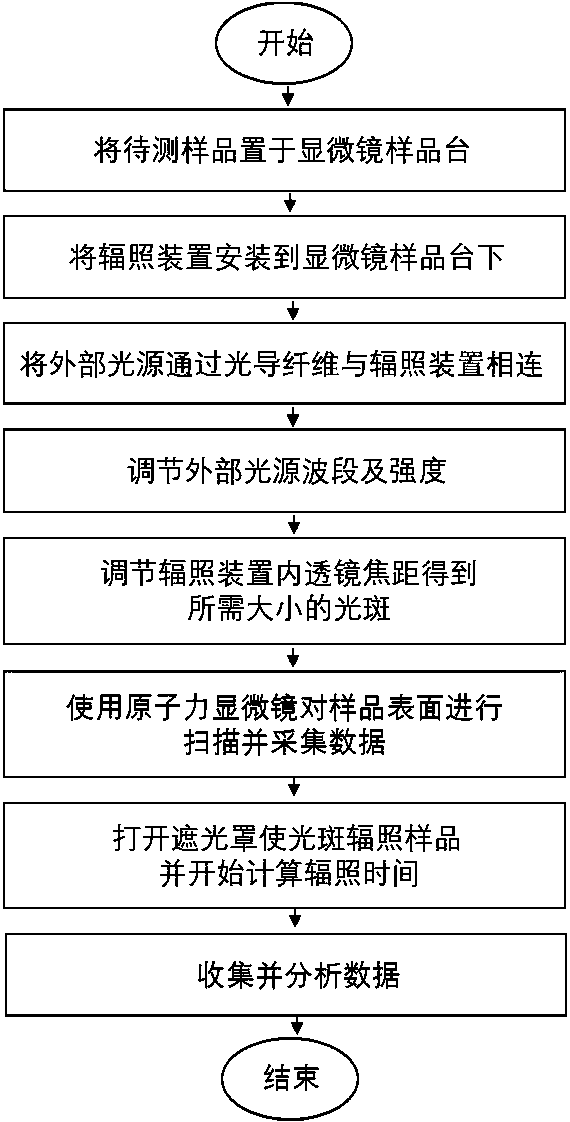
[0028] In embodiment 1, the method for measuring the surface morphology and modulus of elasticity of polylactic acid film under 355nm ultraviolet band irradiation for 5 minutes, the flow process is as follows figure 2 As shown, it specifically includes the following steps:

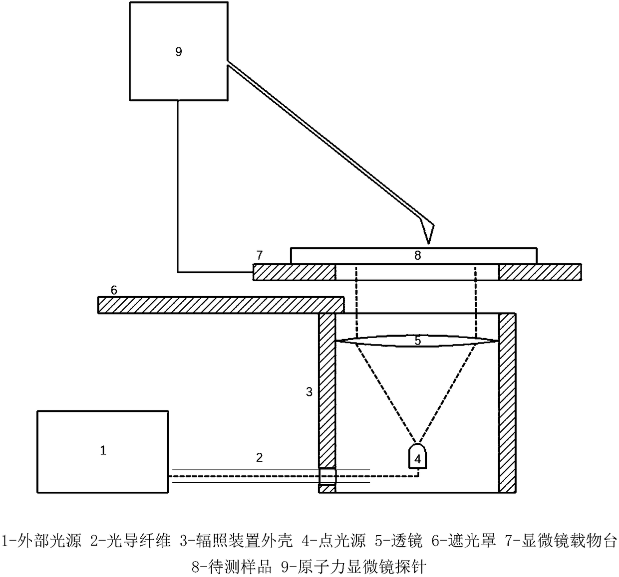
[0029] (1) if figure 1 As shown, the light irradiation device 3 is connected with the atomic force microscope 9 as shown in the figure, and a 2×2 cm polylactic acid film 8 is fixed on the microscope stage 7 . The external light source 1 emits 355nm ultraviolet light, which is transmitted to the light-emitting head 4 through the optical fiber 2, and the beam spreads upward in a point-like manner, and is restrained by the lens 5 to form parallel light;

[0030] (2) Set the atomic force microscope to the contact mode, use a conventional probe to continuously scan the polylactic acid film, and open the light shield 6 to start the experiment until irradiated for 5 minutes. Through software synthesis and anal...

Embodiment 2

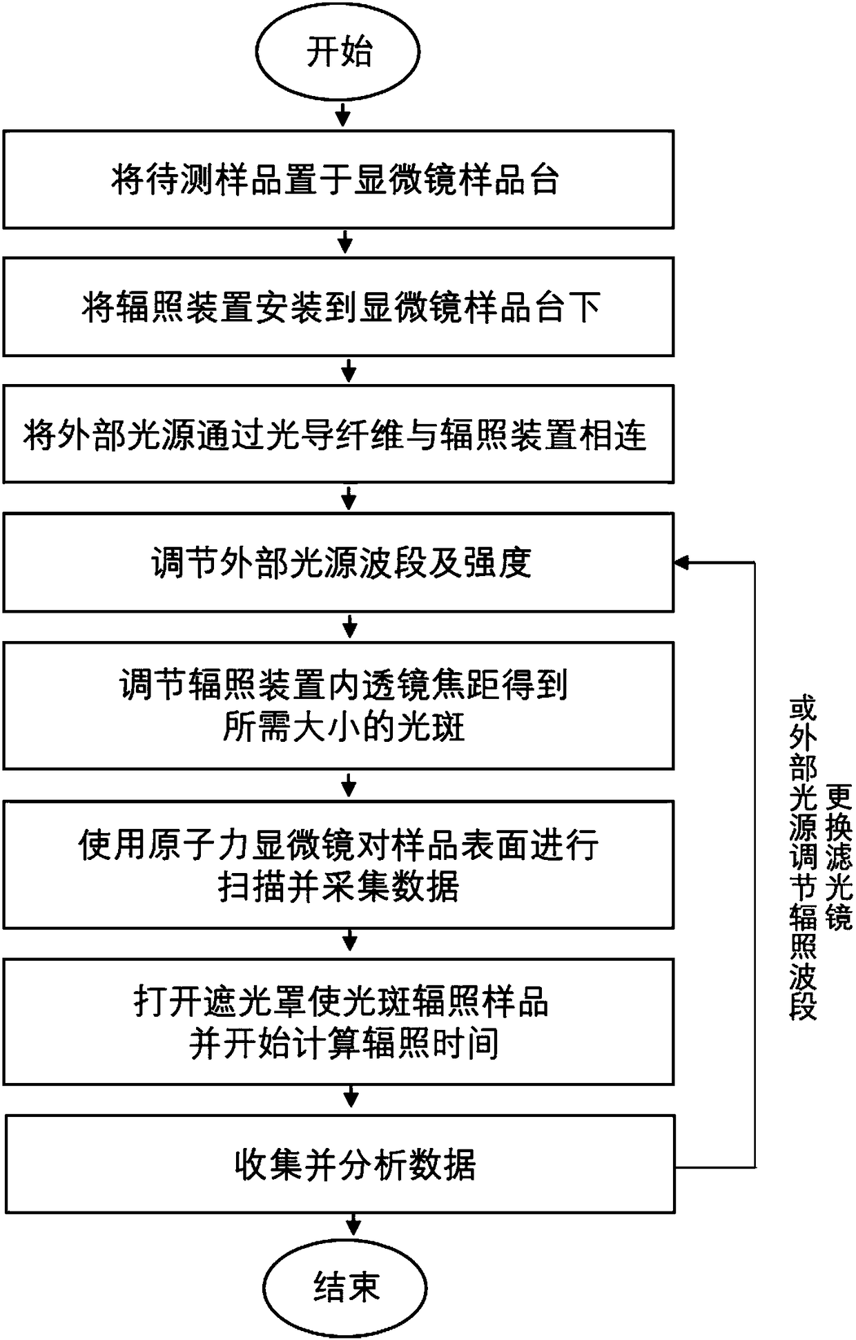
[0033] In embodiment 2, the method for measuring the surface morphology and modulus of elasticity of polylactic acid film under 488nm, 546nm, 800nm ​​band irradiation for 5 minutes, the flow process is as follows image 3 As shown, it specifically includes the following steps:

[0034] (1) if figure 1 As shown in the figure, the light irradiation device was connected with the atomic force microscope as shown in the figure, and a 2×2cm polylactic acid film (referred to as group A1) was fixed on the microscope stage. Connect the visible light external light source and adjust the filter to emit 488nm visible light, which is transmitted to the light-emitting head through the optical fiber, and the beam spreads upward in a point-like manner, and is restrained by the lens to become parallel light;

[0035] (2) Set the atomic force microscope to the contact mode, and use a conventional probe to scan the polylactic acid film continuously until it is irradiated for 5 minutes. After s...

Embodiment 3

[0042] In embodiment 3, the method for measuring the real-time changes in surface morphology, electrical resistance and thermal resistance of a single crystal silicon thin film under 488nm band irradiation for 5 minutes, the process is as follows Figure 4 As shown, it specifically includes the following steps:

[0043] (1) if figure 1 As shown in the figure, the light irradiation device was connected with the atomic force microscope as shown in the figure, and a 2×2 cm single crystal silicon film (recorded as group B1) was fixed on the microscope stage. Connect the visible light external light source and adjust the filter to emit 488nm visible light, which is transmitted to the light-emitting head through the optical fiber, and the beam spreads upward in a point-like manner, and is restrained by the lens to become parallel light;

[0044](2) Set the atomic force microscope to the contact mode, and use a conventional probe to scan the single crystal silicon film continuously ...


PUM


Abstract

The present invention discloses a device based on an atomic force microscope. The device is capable of measuring surface force, electrical, magnetic and thermal properties of sample materials in a special wave band light irradiation condition in real time. The device system is mainly formed by an irradiation device, an external light source and light-guide fibers. The irradiation device is formedby a housing, a point light source, a lens and a lens hood. When used, the irradiation device portion is installed under an objective table for cooperation with the atomic force microscope, the external light source emits an incident beam with special wavebands (ultraviolet, visible light and infrared), the beam is conducted to the point light source in the irradiation device through the light-guide fibers and is diffused upwards in the point shape, and divergent light is restrained by the lens to become parallel light to irradiate the surface of a material sample. The device system is independent of a laser system of the atomic force microscope and has no interference with the laser system of the atomic force microscope, the device employs different external light sources or modes of installing optical filters to regulate the irradiation wavebands, and real-time detection of a plurality of property indexes such as force, electrical, magnetic and thermal properties of samples is achieved through replacement of an atomic force microscope scanning probe module and a mode of a software scheme. Compared to a current test method, the device provided by the invention can accurately reflect the change conditions of the correlation property indexes of the materials in the irradiation process.

Description

technical field [0001] The invention belongs to the technical field of material surface morphology and force, electricity, magnetism and thermal performance testing, and specifically relates to a multi-band sample irradiation device based on an atomic force microscope. Background technique [0002] The surface morphology and mechanical, electrical, magnetic, and thermal properties of materials will change to varying degrees under irradiation in different wavelength bands. Specifically, when polymer materials are irradiated in the ultraviolet band (100-400nm), due to the relatively concentrated energy of the short wavelength of ultraviolet light, the covalent bonds in the molecular chain segments can be broken to reduce the molecular weight of the material, resulting in surface erosion of the material and mechanical damage. Performance decline; photovoltaic materials show different electromagnetic properties due to photoelectric effect or photochemical effect under visible li...

Claims


Application Information

Patent Timeline
IPC IPC(8): G01Q30/20
CPCG01Q30/20
Inventor 王丽珍樊瑜波靳凯翔李林昊王亚伟
Owner BEIHANG UNIV
Why Eureka
Try Eureka