Graphene vertical heterojunction device and preparation method thereof

A heterojunction, graphene technology, applied in semiconductor/solid-state device manufacturing, semiconductor devices, electrical components, etc., can solve problems affecting device performance, affecting device interface flatness, etc., to achieve flexible preparation, compact structure, and anti-oxidation. Effect

Active Publication Date: 2018-08-31
NAT UNIV OF DEFENSE TECH
View PDF5 Cites 2 Cited by
  • Summary
  • Abstract
  • Description
  • Claims
  • Application Information

AI Technical Summary

Problems solved by technology

If the graphene transfer method is used to transfer graphene to the prepared underlying material, the underlying material will inevitably be exposed, resulting in oxidation or surface adsorption. Oxidation in the environment directly affects the performance of the device; if graphene is grown directly on the underlying material substrate, it will face the difficulty of solving the low-temperature growth of multi-substrate graphene, such as: directly preparing graphene on metal materials at high temperature, high temperature Leads to the recrystallization of the metal film, forming a granular structure, which affects the flatness of the interface of the device

Method used


Image

  • Graphene vertical heterojunction device and preparation method thereof
  • Graphene vertical heterojunction device and preparation method thereof
  • Graphene vertical heterojunction device and preparation method thereof

Examples


Embodiment 1

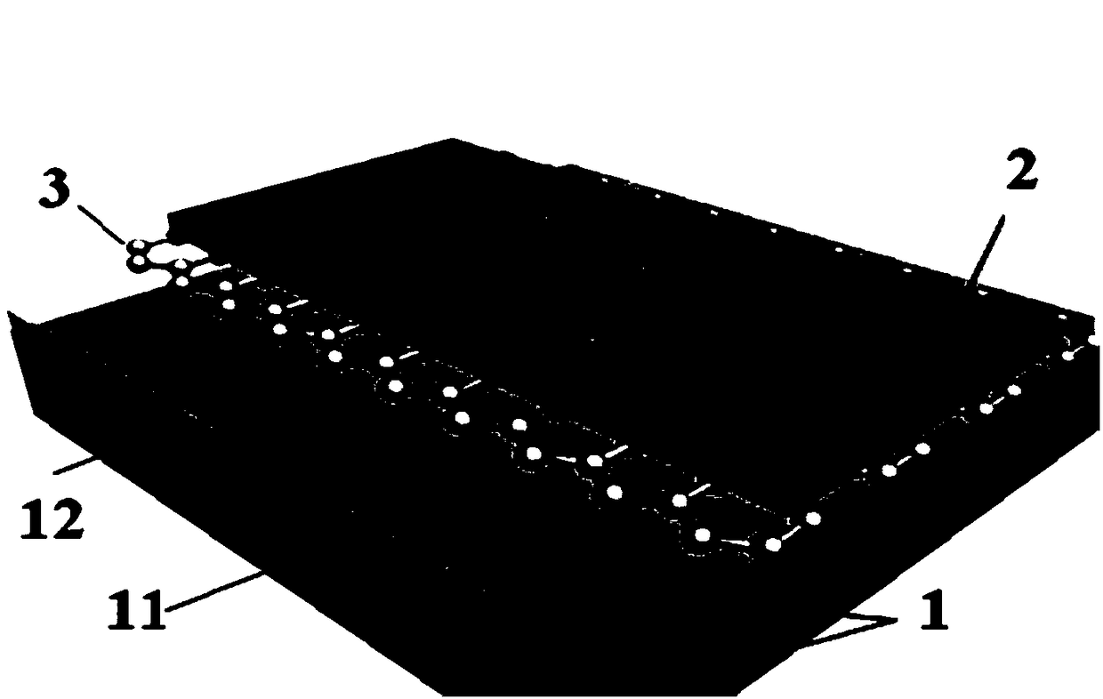
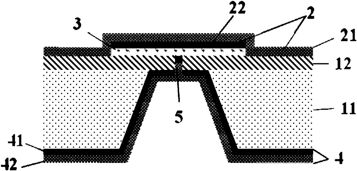
[0040] A graphene vertical heterojunction device of the present invention, specifically a graphene tunnel junction device, such as figure 1 and 2 As shown, it includes a support substrate 1 with nanometer through holes 5 (specifically, a square hole of 910nm×490nm), a graphene layer 3 and a front structural functional layer 2 arranged on the upper surface of the support substrate 1 in sequence, and a nano The back structural functional layer 4 , the front structural functional layer 2 and the rear structural functional layer 4 in the through hole 5 are all physically combined with the graphene layer 3 to form a magnetic tunnel junction.

[0041] In this embodiment, the front structural functional layer 2 includes a front magnetic material layer 22 and a front electrode layer 21 disposed on the upper surface of the front magnetic material layer 22, and the rear structural functional layer 4 includes a rear magnetic material layer 41 and a magnetic material layer disposed on the...


PUM

PropertyMeasurementUnit
diameteraaaaaaaaaa
thicknessaaaaaaaaaa
thicknessaaaaaaaaaa

Abstract

The invention discloses a graphene vertical heterojunction device and a preparation method thereof. The graphene vertical heterojunction device is composed of a graphene layer, a first heterogeneous layer and a support substrate having a through hole. The graphene layer is arranged on the surface of the support substrate; the first heterogeneous layer is arranged in the through hole and is combined with the graphene layer physically to form the first heterojunction. In addition, the preparation method includes the following steps: step one, opening a through hole perpendicular to the surface of a support substrate in the support substrate; step two, transferring suspended graphene to the surface of the support substrate; and step three, preparing a first heterogeneous layer in the throughhole formed in the support substrate. With the method disclosed by the invention, problems of interface oxidation, adsorption and unevenness during traditional preparation process of the graphene vertical device can be solved; and the prepared vertical heterojunction device has advantages of low resistance, good anti-oxidation performance, flat interface, compact structure and low cost and the like.

Description

technical field [0001] The invention belongs to the technical field of preparation of two-dimensional material micro-nano electronic devices, and in particular relates to a graphene vertical heterojunction device and a preparation method thereof. Background technique [0002] Graphene is a honeycomb crystal with a single atomic layer thickness, and it is a new type of nanomaterial with unique properties and broad application prospects. Electronic devices, optical devices, and spin devices prepared using graphene exhibit excellent electrical, optical, and magnetoresistance properties, and are an effective way to realize a new generation of smart chips and sensor chips. In many applications, new types of graphene devices can be constructed by using the weak vertical conductivity of graphene and the novel interface effects of graphene / metal, graphene / ferromagnetism, and graphene / semiconductor, such as metal / graphene / nitrogen Boron / graphene / metal can realize negative differenti...

Claims


Application Information

Patent Timeline
Patent Type & Authority Applications(China)
IPC IPC(8): H01L29/739H01L29/267H01L21/331
CPCH01L29/267H01L29/66356H01L29/7391
Inventor 李裴森潘孟春彭俊平邱伟成胡悦国陈棣湘胡佳飞田武刚张琦
Owner NAT UNIV OF DEFENSE TECH
Why Eureka
Try Eureka