Temporary bound/de-bound material and preparation method and application thereof

A temporary bonding and debonding technology, used in semiconductor/solid-state device manufacturing, electrical components, electrical solid-state devices, etc., can solve the problems of non-reusable, high cost, incomplete temporary bonding glue debonding, etc.

Active Publication Date: 2018-09-07
GUANGDONG UNIV OF TECH
View PDF6 Cites 2 Cited by
  • Summary
  • Abstract
  • Description
  • Claims
  • Application Information

AI Technical Summary

Problems solved by technology

[0005] In view of this, the temporary bonding / debonding material provided by the present invention and its preparation method and application can effectively solve the technical defects of incomplete debonding, non-reusable and high cost of temporary bonding glue

Method used


Image

  • Temporary bound/de-bound material and preparation method and application thereof
  • Temporary bound/de-bound material and preparation method and application thereof
  • Temporary bound/de-bound material and preparation method and application thereof

Examples


preparation example Construction

[0043] The present invention also discloses a method for preparing temporarily bonded / debonded materials, comprising the following steps:

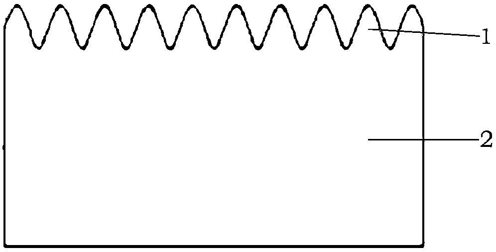
[0044] Step 1: Roughen the surface of the slide to obtain a roughened slide;

[0045] Step 2: attaching the graphite-based material to the rough surface of the roughened slide to obtain a temporarily bonded / debonded material.

[0046] Specifically, step 1 includes performing roughening treatment on the surface of the slide by chemical method or plasma etching method to obtain a roughened slide.

[0047] Specifically, step 2 includes attaching the graphite-based material to the rough surface of the roughened carrier by chemical vapor deposition or magnetron sputtering to obtain a temporarily bonded / debonded material.

[0048] The present invention also discloses the application of temporary bonding / debonding materials in wafer processing, including the following steps:

[0049] Step 1: Electroplating a metal layer on the surface of the wa...

Embodiment 1

[0065] The specific embodiment of the present invention provides a kind of temporarily bonded / unbonded material and its preparation method and application, and embodiment 1 comprises the following steps:

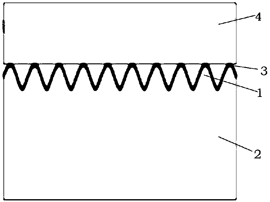
[0066] Step 1: Take an 8-inch silicon wafer, the thickness of the silicon wafer is 100 microns, and the front side of the silicon wafer is coated with a layer of 1 micron copper;

[0067] Step 2: Take a piece of glass as a slide, the thickness of the glass is 30 microns, and the diameter of the glass is the same as that of the silicon wafer;

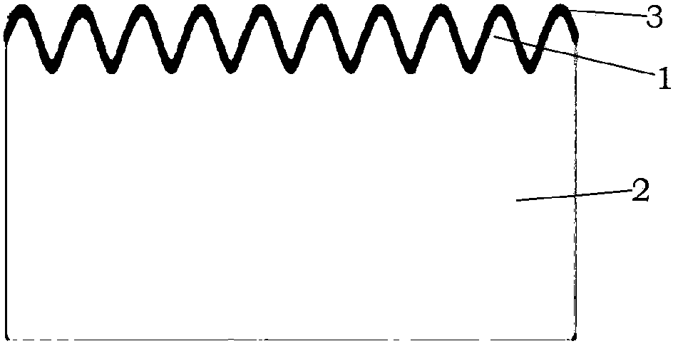
[0068] Step 3: Form a layer of raised microstructure on the glass slide by photochemical etching, the height of the microstructure is 10 microns;

[0069] Step 4: the microstructure of the glass slide is plated with graphite by CVD, and the thickness of the graphite is 5 microns;

[0070] Step 5: temporarily bonding the copper-plated side of the silicon wafer to the graphite layer of the glass slide to obtain a temporary silicon wafer...

Embodiment 2

[0074] The specific embodiment of the present invention provides a kind of temporarily bonded / unbonded material and its preparation method and application, embodiment 2 comprises the following steps:

[0075] Step 1: Take an 8-inch gallium nitride wafer, the thickness of the gallium nitride is 700 microns, and the front side of the gallium nitride is coated with a layer of 1 micron gold;

[0076] Step 2: Take a piece of copper foil as a carrier, the thickness of the copper foil is 30 microns, and the diameter of the copper foil is 1 mm larger than that of gallium nitride;

[0077] Step 3: forming a layer of raised microstructure on the copper foil carrier by wet etching, the height of the microstructure is 15 microns;

[0078] Step 4: The raised structure of the copper foil carrier is plated with graphite by CVD, and the thickness of the graphite is 8 microns;

[0079] Step 5: temporarily bonding the gold-plated side of the gallium nitride wafer to the graphite layer of the c...


PUM

PropertyMeasurementUnit
thicknessaaaaaaaaaa
heightaaaaaaaaaa
thicknessaaaaaaaaaa

Abstract

The invention belongs to the technical field of the semiconductor, and especially relates to a temporary bound/de-bound material and a preparation method and application thereof. The temporary bound/de-bound material provided by the invention comprises roughened slide glass and a graphite material, and the graphite material is attached to a rough surface of the roughened slide glass. The inventionfurther provides a preparation method of the temporary bound/de-bound material, and the preparation method comprises the following steps: performing roughening treatment on the surface of the slide glass to obtain the roughened slide glass; and attaching the graphite material to the rough surface of the roughened slide glass to obtain the temporary bound/de-bound material. Through the material disclosed by the invention, the technical defect that the temporary bonding glue is incomplete in de-binding, free from reuse and high in cost can be solved.

Description

technical field [0001] The invention belongs to the technical field of semiconductors, and in particular relates to a temporary bonding / unbonding material, a preparation method and an application thereof. Background technique [0002] As people's requirements for electronic products are developing in the direction of miniaturization, electronic chips are also developing in a thinner and thinner direction. However, if the thickness of silicon wafers is to be reduced to 100 μm or less, it is very easy to cause debris, or It is because the wafer is bent and deformed due to stress during the processing of the wafer, so it is impossible to directly process such an ultra-thin wafer. Therefore, in order to be able to process this type of ultra-thin wafer, it is necessary to temporarily bond this ultra-thin functional wafer to a carrier wafer first, and after bonding, the functional wafer and the carrier wafer are bonded together , the thinning of functional wafers, the manufacture...

Claims


Application Information

Patent Timeline
Patent Type & Authority Applications(China)
IPC IPC(8): H01L21/683H01L21/603
CPCH01L21/6835H01L24/81H01L24/98H01L2224/81005H01L2224/98
Inventor 崔成强张昱陈涛陈新
Owner GUANGDONG UNIV OF TECH
Why Eureka
Try Eureka