Temporarily bonded/debonded materials, methods of preparation and applications thereof
A temporary bonding and debonding technology, which is applied in semiconductor/solid-state device manufacturing, semiconductor devices, electrical components, etc., can solve the problems of incomplete temporary bonding, unrepeatable bonding, high cost, etc.
- Summary
- Abstract
- Description
- Claims
- Application Information
AI Technical Summary
Problems solved by technology
Method used
Image
Examples
preparation example Construction
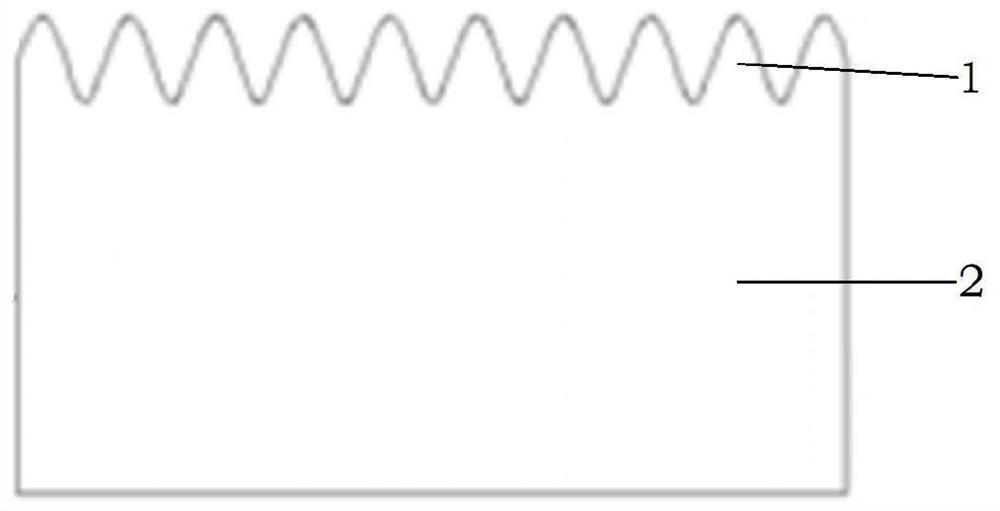
[0043] The present invention also discloses a method for preparing temporarily bonded / debonded materials, comprising the following steps:
[0044] Step 1: Roughen the surface of the slide to obtain a roughened slide;
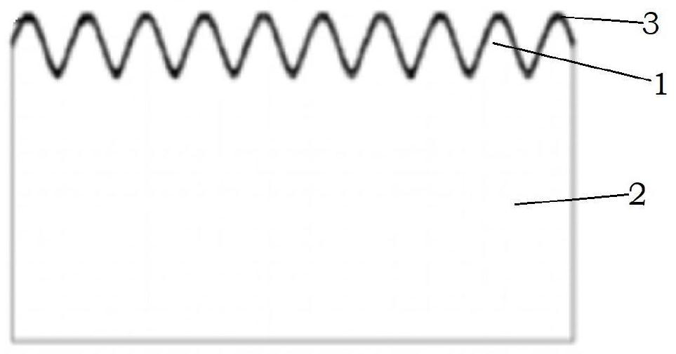
[0045] Step 2: attaching the graphite-based material to the rough surface of the roughened slide to obtain a temporarily bonded / debonded material.
[0046] Specifically, step 1 includes performing roughening treatment on the surface of the slide by chemical method or plasma etching method to obtain a roughened slide.
[0047] Specifically, step 2 includes attaching the graphite-based material to the rough surface of the roughened carrier by chemical vapor deposition or magnetron sputtering to obtain a temporarily bonded / debonded material.
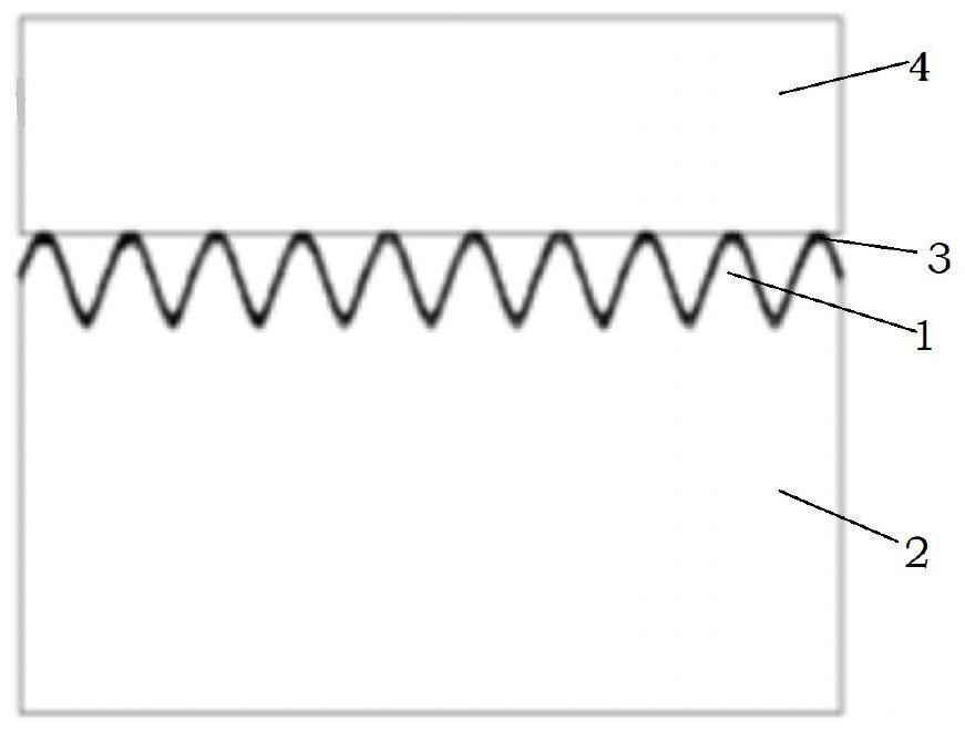
[0048] The present invention also discloses the application of temporary bonding / debonding materials in wafer processing, including the following steps:
[0049] Step 1: Electroplating a metal layer on the surface of the wa...
Embodiment 1
[0065] The specific embodiment of the present invention provides a kind of temporarily bonded / unbonded material and its preparation method and application, and embodiment 1 comprises the following steps:
[0066] Step 1: Take an 8-inch silicon wafer, the thickness of the silicon wafer is 100 microns, and the front side of the silicon wafer is coated with a layer of 1 micron copper;
[0067] Step 2: Take a piece of glass as a slide, the thickness of the glass is 30 microns, and the diameter of the glass is the same as that of the silicon wafer;
[0068] Step 3: Form a layer of raised microstructure on the glass slide by photochemical etching, the height of the microstructure is 10 microns;
[0069] Step 4: the microstructure of the glass slide is plated with graphite by CVD, and the thickness of the graphite is 5 microns;
[0070] Step 5: temporarily bonding the copper-plated side of the silicon wafer to the graphite layer of the glass slide to obtain a temporary silicon wafer...
Embodiment 2
[0074] The specific embodiment of the present invention provides a kind of temporarily bonded / unbonded material and its preparation method and application, embodiment 2 comprises the following steps:
[0075] Step 1: Take an 8-inch gallium nitride wafer, the thickness of the gallium nitride is 700 microns, and the front side of the gallium nitride is coated with a layer of 1 micron gold;
[0076] Step 2: Take a piece of copper foil as a carrier, the thickness of the copper foil is 30 microns, and the diameter of the copper foil is 1 mm larger than that of gallium nitride;
[0077] Step 3: forming a layer of raised microstructure on the copper foil carrier by wet etching, the height of the microstructure is 15 microns;
[0078] Step 4: The raised structure of the copper foil carrier is plated with graphite by CVD, and the thickness of the graphite is 8 microns;
[0079] Step 5: temporarily bonding the gold-plated side of the gallium nitride wafer to the graphite layer of the c...
PUM
| Property | Measurement | Unit |
|---|---|---|
| height | aaaaa | aaaaa |
| thickness | aaaaa | aaaaa |
| height | aaaaa | aaaaa |
Abstract
Description
Claims
Application Information


