Ultra-thick 5G antenna PCB module processing method

A module processing, 5G technology, applied in the processing of insulating substrates/layers, multi-layer circuit manufacturing, electrical components, etc., can solve problems such as time-consuming, accuracy deviation, and signal debugging difficulties, and improve accuracy and product quality , prevent precision deviation, reduce the effect of process difficulty

Active Publication Date: 2018-09-07
HUIZHOU KING BROTHER CIRCUIT TECH +2
View PDF7 Cites 12 Cited by
  • Summary
  • Abstract
  • Description
  • Claims
  • Application Information

AI Technical Summary

Problems solved by technology

[0005] The traditional method of antenna module is to use injection molding process, but due to precision deviation and process limitations, signal debugging after installation is difficult and takes a lot o

Method used


Image

  • Ultra-thick 5G antenna PCB module processing method
  • Ultra-thick 5G antenna PCB module processing method

Examples


Embodiment Construction

[0034] In order to enable those skilled in the art to better understand the technical solutions of the present invention, the present invention will be further described in detail below in conjunction with the embodiments and accompanying drawings.

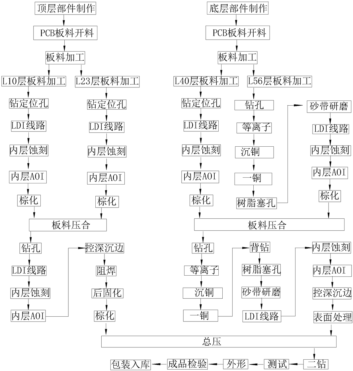
[0035] Such as figure 1 As shown, a processing method for an ultra-thick 5G antenna PCB module includes the following processing steps:

[0036] Step 1: Top layer parts making:

[0037] Step 1.1, material cutting: Cutting the PCB substrate according to the design structure, that is, two inner layer materials of L10 and L23;

[0038] Step 1.2, sheet material processing: the L10 layer sheet material and the L23 layer sheet material are respectively subjected to drilling positioning holes, LDI lines, inner layer etching, inner layer AOI, and browning treatment;

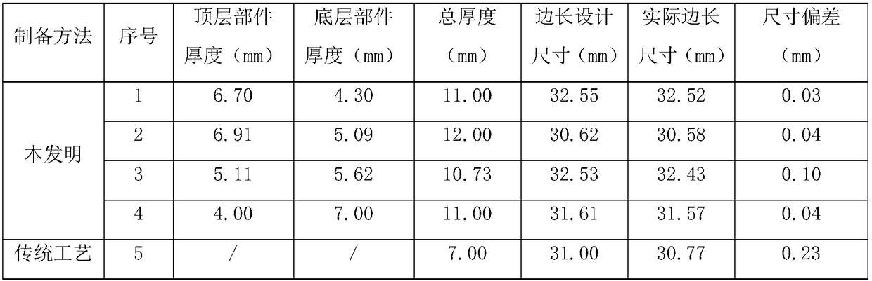
[0039] Step 1.3, sheet pressing: press the L10 layer sheet and the L23 layer sheet processed in step 1.2 to obtain the L13 layer sheet, the thickness of the L13 layer sheet ...


PUM

PropertyMeasurementUnit
Thicknessaaaaaaaaaa

Abstract

The present invention discloses an ultra-thick 5G antenna PCB module processing method. The method comprises the following steps: (1) manufacturing a top layer part; (2) manufacturing a bottom layer part; and (3) manufacturing a finished product. The manufacture of the top layer part and the manufacture of the bottom layer part both comprise cutting, plate material processing and plate material pressing. According to the method, by optimizing the structure and the preparation process of an ultra-thick 5G antenna PCB module, the process difficulty is reduced, the machinable plate thickness reaches to 7-12 mm, the circuit, electroplating and etching requirement(s) of an ultra-thick plate can be effectively satisfied by using a conventional device, the preparation precision of the product isimproved, so that the shape deviation of the finished product is small, and thus the yield rate of the product is improved.

Description

technical field [0001] The invention relates to the technical field of manufacturing 5G communication printed circuit boards, in particular to a processing method for an ultra-thick 5G antenna PCB module. Background technique [0002] As the fifth-generation mobile communication technology, 5G network has a theoretical maximum transmission speed of up to 10Gb per second, which is hundreds of times faster than the current 4G network transmission speed; due to its high speed, low delay, and low power consumption, In the future, it will penetrate into the Internet of Things and all walks of life, and deeply integrate with industrial facilities, medical equipment, transportation, etc., to effectively meet the diversified business needs of vertical industries such as industry, medical care, and transportation. [0003] In order to seize the future market, many countries and regions attach great importance to 5G commercial use, and have started to develop 5G network technology. T...

Claims


Application Information

Patent Timeline
IPC IPC(8): H05K3/46
CPCH05K3/4611H05K2203/0214H05K3/0047H05K3/0052H05K3/4623H05K2203/0278H05K2201/10098H05K2203/0228
Inventor 唐宏华武守坤陈春林映生卫雄范思维石学兵
Owner HUIZHOU KING BROTHER CIRCUIT TECH
Why Eureka
Try Eureka