Method for utilizing ultraviolet light to activate bonded glass and other materials arranged in a stacked manner
An ultra-violet, superimposed technology, applied in electrical components, semiconductor/solid-state device manufacturing, circuits, etc., can solve the problems of being easily interfered by human factors, low activation efficiency, etc., to improve activation efficiency, improve bonding quality, Reduce the effect of adsorption
- Summary
- Abstract
- Description
- Claims
- Application Information
AI Technical Summary
Problems solved by technology
Method used
Image
Examples
Embodiment 1
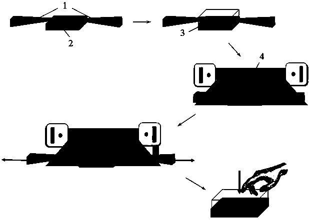
[0025] This embodiment provides a method for bonding stacked glass and other materials using the ultraviolet light activation method, such as figure 1 As shown, the specific implementation steps are as follows:
[0026] (1) Clean the material to be bonded and the wedge:
[0027] Soak the glass wafers, silicon carbide wafers and two wedge-shaped wafers with a length of 15mm, a width of 5mm and a thickness of 0.5mm in deionized water, all of which are 10×10×0.5mm in size, and perform ultrasonic cleaning for 10 minutes. Stream to dry.
[0028] (2) Place the wedge-shaped piece:
[0029] Take two wedges of the above size and place them on the edge of the silicon carbide wafer.
[0030] (3) Place the glass wafer:
[0031] The cleaned glass wafer on the side to be bonded is opposed to the silicon carbide wafer on the side to be bonded and placed above the wedge-shaped wafer.
[0032] (4) Activate the wafer pair to be bonded:
[0033] Place the silicon carbide wafer and glass wafer pair to be bon...
Embodiment 2
[0039] This embodiment provides a method for bonding stacked glass and other materials by using the ultraviolet light activation method. The specific implementation steps are as follows:
[0040] (1) Clean the material to be bonded and the wedge:
[0041] Soak the glass wafers, silicon wafers and two wedge-shaped wafers with a length of 15mm, a width of 5mm and a thickness of 0.5mm in deionized water, which are all 10×10×0.5mm in size, and perform ultrasonic cleaning for 10 minutes. Blow dry.
[0042] (2) Place the wedge-shaped piece:
[0043] Take two wedges of the above size and place them on the edge of the silicon wafer.
[0044] (3) Place the glass wafer:
[0045] The cleaned glass wafer on the side to be bonded is opposed to the silicon wafer on the side to be bonded and placed above the wedge.
[0046] (4) Activate the wafer pair to be bonded:
[0047] Place the silicon wafer and glass wafer pair to be bonded at a distance of 1 mm directly below the ultraviolet light source (the di...
PUM
| Property | Measurement | Unit |
|---|---|---|
| thickness | aaaaa | aaaaa |
| thickness | aaaaa | aaaaa |
| width | aaaaa | aaaaa |
Abstract
Description
Claims
Application Information


