LED epitaxial structure and growth method therefor

A technology of epitaxial growth and growth temperature, which is applied in the direction of electrical components, circuits, semiconductor devices, etc., can solve the problems of increasing the recombination efficiency of holes and electrons in the light-emitting layer, and increasing the high optical power, so as to improve the level of hole injection and reduce the working voltage , Improve the effect of activation efficiency

Active Publication Date: 2017-03-22
XIANGNENG HUALEI OPTOELECTRONICS
View PDF5 Cites 14 Cited by
  • Summary
  • Abstract
  • Description
  • Claims
  • Application Information

AI Technical Summary

Problems solved by technology

High optical efficiency means high optical power and low driving voltage, but the optical power is limited by the hole concentration of the P layer to a certain extent, and the driving voltage is limited by the hole mobility of the P layer to a certain extent. The recombination efficiency of holes and electrons in the layer increases, the high optical power increases, and the hole mobility of the P layer increases to reduce the driving voltage.

Method used


Image

  • LED epitaxial structure and growth method therefor
  • LED epitaxial structure and growth method therefor
  • LED epitaxial structure and growth method therefor

Examples


Embodiment 1

[0049] The invention uses VEECO MOCVD to grow high-brightness GaN-based LED epitaxial wafers. Using high-purity H 2 or high purity N 2 or high purity H 2 or high purity N 2 (purity 99.999%) mixed gas as carrier gas, high-purity NH3 (NH3 purity 99.999%) as N source, metal-organic source trimethylgallium (TMGa), metal-organic source triethylgallium (TEGa), trimethyl Indium (TMIn) is used as the indium source, trimethylaluminum (TMAl) is used as the aluminum source, the N-type dopant is silane (SiH4), the P-type dopant is dichloromagnesium (Cp2Mg), and the substrate is (0001) plane For sapphire, the reaction pressure is between 100Torr and 1000Torr. The specific growth method is as follows (for the epitaxial structure, please refer to figure 2 ):

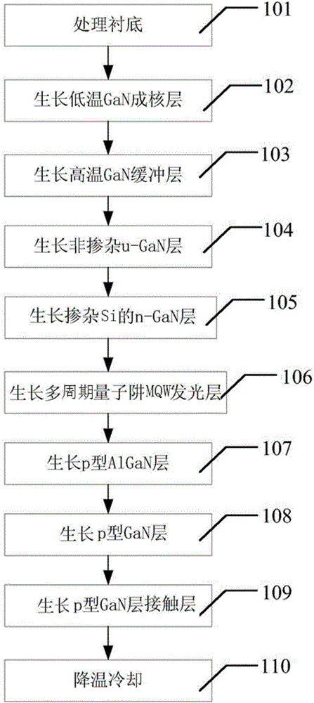
[0050] The present invention provides an LED epitaxial structure and its growth method, see image 3 , which in turn includes:

[0051] Step 1, processing the substrate 101; Step 2, growing a low-temperature GaN nucleation lay...

Embodiment 2

[0058] The invention uses VEECO MOCVD to grow high-brightness GaN-based LED epitaxial wafers. Using high-purity H 2 or high purity N 2 or high purity H 2 or high purity N 2 (purity 99.999%) mixed gas as carrier gas, high-purity NH3 (NH3 purity 99.999%) as N source, metal-organic source trimethylgallium (TMGa), metal-organic source triethylgallium (TEGa), trimethyl Indium (TMIn) is used as the indium source, trimethylaluminum (TMAl) is used as the aluminum source, the N-type dopant is silane (SiH4), the P-type dopant is dichloromagnesium (Cp2Mg), and the substrate is (0001) plane For sapphire, the reaction pressure is between 100Torr and 1000Torr. The specific growth method is as follows (for the epitaxial structure, please refer to figure 2 ):

[0059] 1. Treat the substrate, specifically:

[0060] Place the sapphire substrate in H 2 Annealing is carried out in the atmosphere to clean the surface of the substrate, and the temperature is 1050°C-1150°C.

[0061] 2. Gro...


PUM


Abstract

The invention aims to provide an LED epitaxial structure and a growth method therefor. The growth method specifically comprises the steps of processing a substrate, enabling a low-temperature GaN core-forming layer, a high-temperature GaN buffer layer, a non-doped u-GaN layer, a Si-doped n-GaN layer, a multi-period quantum well (MQW) light emitting layer, a P type AlGaN layer, a P type GaN layer and a P type GaN contact layer to be grown, and then reducing temperature and cooling, wherein the step of growing a p type GaN layer is performed by the steps of enabling the P type GaN layer to be grown at a low temperature in N<2> atmosphere firstly, then enabling the P type GaN layer to be grown at a high temperature in H<2> atmosphere, and finally enabling the P type GaN layer to be grown at a high temperature in N<2>/H<2> mixed gas so as to lower the working voltage of the LED and improve the light emitting efficiency of the LED. The invention also aims to provide the LED epitaxial structure produced by the growth method for the epitaxial structure; according to the structure, the conventional high-temperature p type GaN layer structure is changed into the p type GaN layer structure with the variable atmospheres of low-temperature N<2> atmosphere, high-temperature H<2> atmosphere and high-temperature N<2>/H<2> mixed gas, so that the problems that the luminous power of the LED is limited by P layer hole concentration and the driving voltage is limited by P layer hole mobility are solved.

Description

technical field [0001] The present application relates to the technical field of LED epitaxial design application, in particular, to an LED epitaxial structure and a growth method thereof. Background technique [0002] At present, LED (Light Emitting Diode, light-emitting diode) is a kind of solid-state lighting. The advantages of small size, low power consumption, long service life, high brightness, environmental protection, and durability are recognized by consumers. The scale of domestic production of LEDs is also gradually expanding; the market The demand for LED brightness and luminous efficiency is increasing day by day. How to grow better epitaxial wafers has been paid more and more attention. Because of the improvement of the quality of epitaxial layer crystals, the performance of LED devices can be improved. The ability and stability will increase with the improvement of the crystal quality of the epitaxial layer. [0003] The traditional LED epitaxial structure gr...

Claims


Application Information

Patent Timeline
Patent Type & Authority Applications(China)
IPC IPC(8): H01L33/00H01L33/12H01L33/20H01L33/22
CPCH01L33/005H01L33/12H01L33/20H01L33/22H01L2933/0008H01L2933/0033
Inventor 林传强
Owner XIANGNENG HUALEI OPTOELECTRONICS
Why Eureka
Try Eureka