Capacitor array structure and manufacturing method thereof

An array structure and capacitor technology, which is applied in the direction of electric solid-state devices, circuits, electrical components, etc., can solve problems such as the decline in the storage capacity of capacitors, the increase in the leakage rate of capacitors, and the decrease in the stability of capacitor electrical connections, so as to improve the stability of electrical connections , reduce the leakage rate, and ensure the effect of charge storage capacity

Pending Publication Date: 2018-09-14
CHANGXIN MEMORY TECH INC
View PDF10 Cites 12 Cited by
  • Summary
  • Abstract
  • Description
  • Claims
  • Application Information

AI Technical Summary

Problems solved by technology

[0005] In view of the above-mentioned shortcomings of the prior art, the object of the present invention is to provide a capacitor array structure and its preparation method, which is used to solve the problem of the formation of the by-product chlorine ion doping

Method used


Image

  • Capacitor array structure and manufacturing method thereof
  • Capacitor array structure and manufacturing method thereof
  • Capacitor array structure and manufacturing method thereof

Examples


Embodiment 1

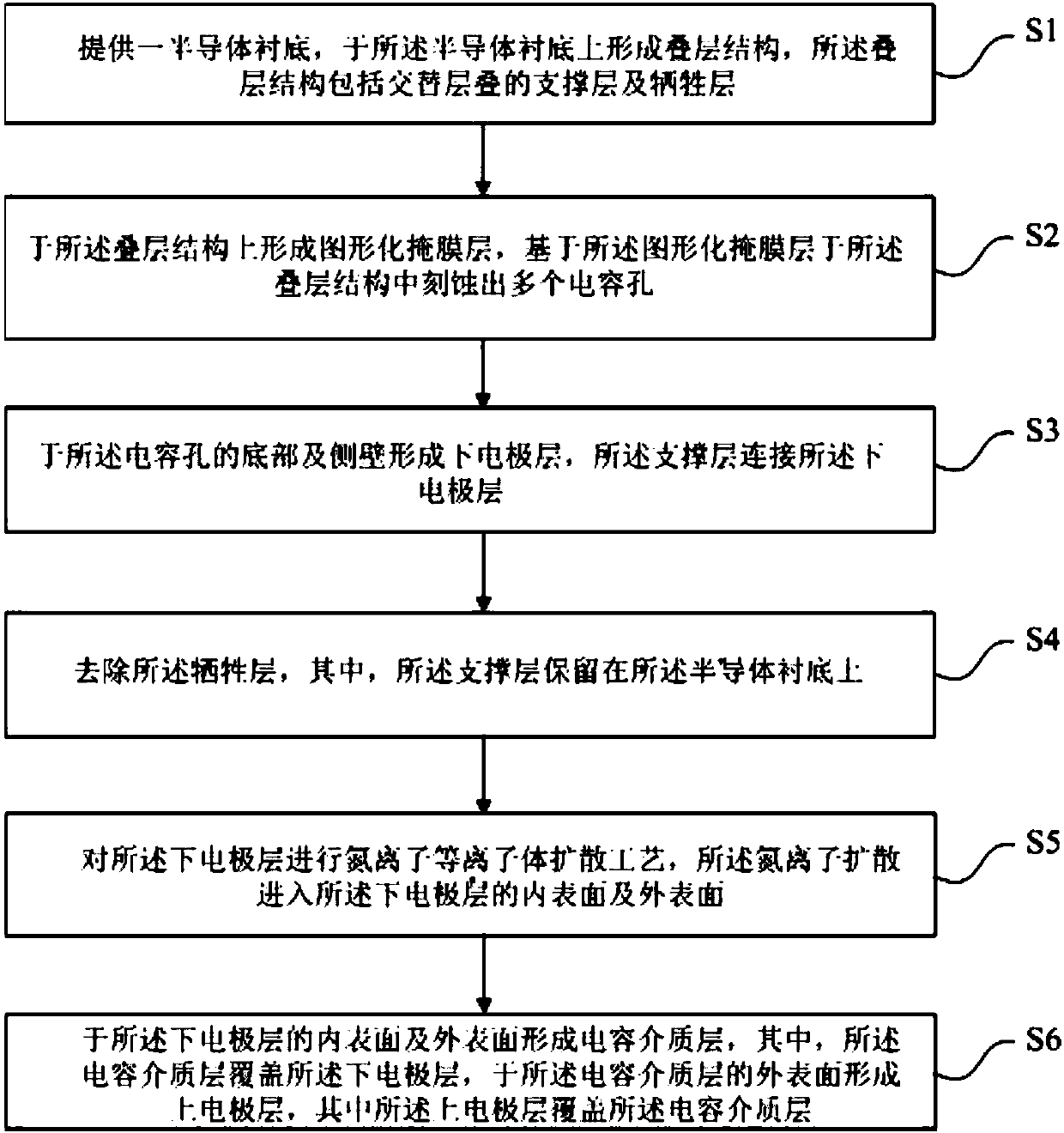
[0115] see figure 2 , the present embodiment provides a method for preparing a capacitor array structure, the method for preparing a capacitor array structure includes the following steps:

[0116] 1) A semiconductor substrate is provided, and a stacked structure is formed on the semiconductor substrate, the stacked structure comprising alternately stacked support layers and sacrificial layers;

[0117] 2) forming a patterned mask layer on the stacked structure, and etching a plurality of capacitance holes in the stacked structure based on the patterned mask layer;

[0118] 3) forming a lower electrode layer on the bottom and side walls of the capacitor hole, and the supporting layer is connected to the lower electrode layer;

[0119] 4) removing the sacrificial layer, wherein the support layer remains on the semiconductor substrate;

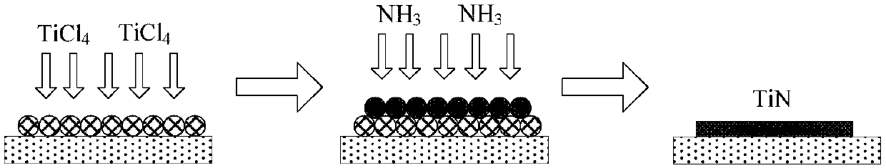
[0120] 5) performing a nitrogen ion plasma diffusion process on the lower electrode layer, and the nitrogen ions diffuse into the inner surf...

Embodiment 2

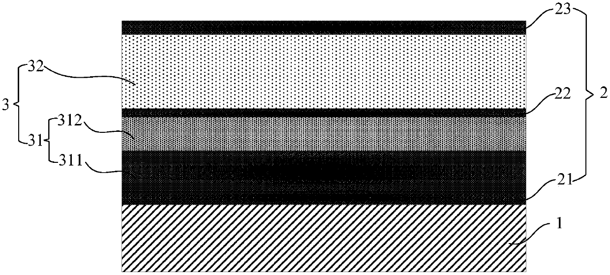
[0163] Please continue to refer to Embodiment 1 Figure 14 , the present invention also provides a capacitor array structure, wherein the capacitor array structure is preferably prepared by the preparation method of the present invention, of course, is not limited thereto, and the capacitor array structure includes:

[0164] semiconductor substrate 1;

[0165] The lower electrode layer 6 is formed on the semiconductor substrate 1, the cross-sectional shape of the lower electrode layer 6 includes a U shape, and the inner surface and the outer surface of the lower electrode layer 6 are diffusely implanted with nitrogen ions;

[0166] a capacitor dielectric layer 7 covering the inner and outer surfaces of the lower electrode layer 6;

[0167] The upper electrode layer 8 covers the outer surface of the capacitor dielectric layer 7 .

[0168] Wherein, the nitrogen ions diffused and implanted on the inner and outer surfaces of the lower electrode layer 6 can squeeze out the impuri...


PUM


Abstract

The invention provides a capacitor array structure and a manufacturing method thereof. The method comprises steps: 1) a semiconductor substrate is provided, and a laminated structure is formed on thesemiconductor substrate; 2) a patterned mask layer is formed on the laminated structure and multiple capacitor holes are etched in the laminated structure based on the patterned mask layer; 3) a lowerelectrode layer is formed on the bottom part and the side wall of the capacitor hole, and a supporting layer is connected with the lower electrode layer; 4) a sacrificial layer is removed; 5) a nitrogen ion plasma diffusion process is carried out on the lower electrode layer, and the nitrogen ions are diffused to the inner surface and the outer surface of the lower electrode layer; and 6) a capacitive dielectric layer is formed on the inner surface and the outer surface of the lower electrode layer and an upper electrode layer is formed on the outer surface of the capacitive dielectric layer.Through carrying out nitrogen ion plasma diffusion process processing on the lower electrode layer, the electrical connection stability and the charge storage capacity of the capacitor can be effectively improved, and the electricity leakage rate of the capacitor is also reduced.

Description

technical field [0001] The invention belongs to the field of semiconductor device manufacturing, in particular to a method for preparing a capacitor array. Background technique [0002] Dynamic Random Access Memory (DRAM for short) is a semiconductor storage device commonly used in computers, and is composed of many repeated storage units. Each memory cell usually includes a capacitor and a transistor; the gate of the transistor is connected to the word line, the drain is connected to the bit line, and the source is connected to the capacitor; the voltage signal on the word line can control the opening or closing of the transistor, and then through the bit line Read the data information stored in the capacitor, or write the data information into the capacitor through the bit line for storage. With the continuous evolution of the DRAM process technology, the integration level continues to increase, and the component size continues to shrink. In the current DRAM process below...

Claims


Application Information

Patent Timeline
IPC IPC(8): H01L27/08H01L29/92
CPCH01L27/0805H01L29/92
Inventor 不公告发明人
Owner CHANGXIN MEMORY TECH INC
Why Eureka
Try Eureka