Shallow trench separation structure, formation method thereof and image sensor

A technology of isolation structure and shallow trench, which is applied in the manufacture of electrical solid-state devices, semiconductor devices, semiconductor/solid-state devices, etc., can solve the problems affecting the performance of semiconductor devices and generating dark current, so as to reduce the surface state density and dark current , high diffusion effect

Inactive Publication Date: 2018-09-18
HUAIAN IMAGING DEVICE MFGR CORP
View PDF4 Cites 3 Cited by
  • Summary
  • Abstract
  • Description
  • Claims
  • Application Information

AI Technical Summary

Problems solved by technology

[0004] However, when the shallow trench isolation structure is used to isolate light-receiving elements such as photodiodes, photoconductive elements, and photoelectric tubes, the shallow trench isolation structures formed in the prior art will generate dark current in the light-receiving elements and affect the performance of semiconductor devices.

Method used


Image

  • Shallow trench separation structure, formation method thereof and image sensor
  • Shallow trench separation structure, formation method thereof and image sensor
  • Shallow trench separation structure, formation method thereof and image sensor

Examples


Embodiment Construction

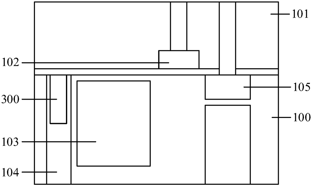
[0022] The shallow trench isolation structure formed by the existing technology is prone to dark current, and the reason is analyzed in conjunction with a CMOS image sensor, such as figure 1 As shown, the CMOS image sensor includes: a semiconductor substrate 100, an interlayer dielectric layer (ILD) 101 and a transfer transistor gate (TX) 102 formed on the semiconductor substrate 100, and a photodiode ( PD) 103 , shallow trench isolation (STI) 300 , isolation region (ISO) 104 and floating diffusion region (FD) 105 .

[0023] The material of the semiconductor substrate 100 can be, for example, silicon (Si), and the filling material of the shallow trench isolation structure 300 can be, for example, silicon oxide (SiO 2 ), the shallow trench isolation structure 300 is used to isolate adjacent pixel regions (Pixel), but the interface of this structure (such as Si-SiO 2 Interface) there are dangling bonds, which will cause a current flowing in the photodiode in the state of no lig...


PUM


Abstract

The invention discloses a shallow trench separation structure, a formation method thereof and an image sensor. The formation method comprises steps of providing a semiconductor substrate, and forminga grinding stopping layer on the semiconductor substrate; successively etching the grinding stopping layer and the semiconductor substrate, and shallow trenches in the grinding stopping layer and thesemiconductor substrate; forming oxide layers on the surface of the grinding stopping layer, side walls of the shallow trenches and the bottom; forming a fluorine-doped medium layer on the surface ofeach oxide layer; filling the interiors of the shallow trench with insulation media, wherein the insulation media fill the shallow trench and cover the fluorine-doped medium layer; and carrying out annealing technology. According to the invention, through the planarization technology, by removing the insulation media, the fluorine-doped medium layer and the oxide layers on the grinding stopping layer, a shallow trench separation structure is formed. Through the shallow trench separation structure, dark current of the image sensor can be reduced.

Description

technical field [0001] The invention relates to the manufacturing field of semiconductor devices, in particular to a shallow trench isolation structure and its forming method, and an image sensor. Background technique [0002] With the development trend of high-density integrated circuits, the devices that make up the circuit are placed more closely in the chip to fit the available space of the chip. Correspondingly, the density of active devices per unit area of ​​the semiconductor substrate continues to increase, so effective insulation between devices becomes more important. [0003] Shallow Trench Isolation (STI) technology has good isolation effects (such as process isolation effect and electrical isolation effect), shallow trench isolation technology also has the advantages of reducing the area occupied by the wafer surface and increasing the integration of devices, etc. advantage. Therefore, with the reduction of the size of integrated circuits, shallow trench isola...

Claims


Application Information

Patent Timeline
Patent Type & Authority Applications(China)
IPC IPC(8): H01L21/762H01L27/146
CPCH01L21/762H01L27/14601
Inventor 何延强林宗德黄仁德李晓明
Owner HUAIAN IMAGING DEVICE MFGR CORP
Why Eureka
Try Eureka