Diode and manufacturing method thereof

A diode and metal anode technology, applied in the field of power semiconductor devices, can solve the problems of reducing forward conduction voltage, poor reverse recovery characteristics, large conduction loss, etc., achieving good breakdown voltage, strong anti-surge current capability, Good forward voltage drop effect

Active Publication Date: 2018-09-18
UNIV OF ELECTRONIC SCI & TECH OF CHINA
View PDF2 Cites 0 Cited by
  • Summary
  • Abstract
  • Description
  • Claims
  • Application Information

AI Technical Summary

Problems solved by technology

[0005] In view of the above, the object of the present invention is to: aim at the problems of large conduction loss and poor reverse recovery characteristics of PIN diodes in the prior art, and propose a method that can reduce the forward conduction voltage and optimize the

Method used


Image

  • Diode and manufacturing method thereof
  • Diode and manufacturing method thereof
  • Diode and manufacturing method thereof

Examples


Embodiment 1

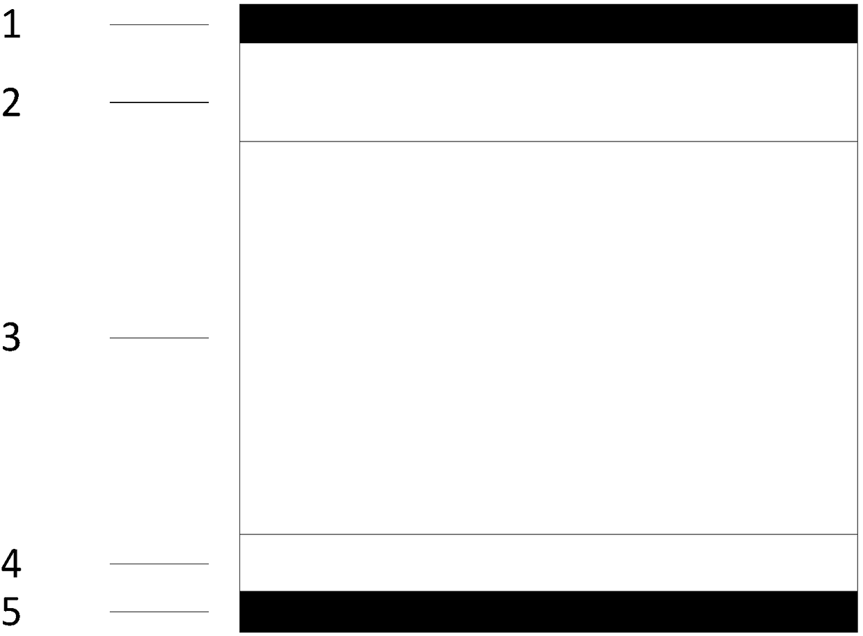
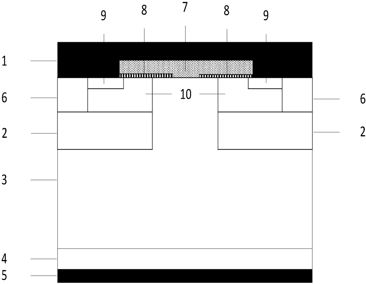
[0074] A diode device with a cell structure such as figure 2 As shown, the bottom-up includes a metal cathode 5, an N+ silicon carbide substrate 4, an N-silicon carbide epitaxial layer 3, and a metal anode 1 stacked in sequence; the top layer of the N-silicon carbide epitaxial layer 3 has a trench structure on both sides The trench structure includes a P+ silicon carbide region 2, a P+ silicon carbide contact region 6, an N+ silicon carbide source region 9 and a P-type silicon carbide Well region 10. The P+ silicon carbide region 2 is located at the bottom of the trench, and the P+ silicon carbide contact region 6 and P-type silicon carbide Well region 10 are located side by side on the upper surface of P+ silicon carbide region 2, N+ silicon carbide source region 9 is located on the top of P-type silicon carbide Well region 10 and in contact with P+ silicon carbide contact region 6; P+ silicon carbide contact region 6 and part of the upper surface of the N+ silicon carbide sou...

Embodiment 2

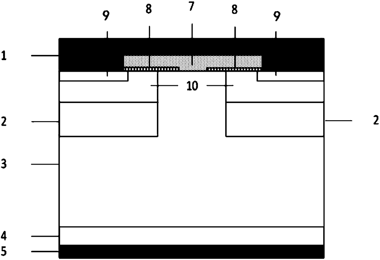
[0084] A diode device with a cell structure such as image 3 As shown, the bottom-up includes a metal cathode 5, an N+ silicon carbide substrate 4, an N-silicon carbide epitaxial layer 3, and a metal anode 1 stacked in sequence; the top layer of the N-silicon carbide epitaxial layer 3 has grooves on both sides The trench structure includes a P+ silicon carbide region 2, an N+ silicon carbide source region 9 and a P-type silicon carbide Well region 10. The P+ silicon carbide region 2 is located at the bottom of the trench, and the P-type silicon carbide Well region 10 is located at the P+ silicon carbide On the upper surface of zone 2, the N+ silicon carbide source region 9 is located on the top of the P-type silicon carbide Well region 10; part of the upper surface of the N+ silicon carbide source region 9 is in contact with the metal anode 1, and part of the N+ silicon carbide source region 9, P-type silicon carbide Well The upper surface of the region 10 and part of the N-sili...

Embodiment 3

[0087] A diode device with a cell structure such as Figure 4 As shown, the bottom-up includes a metal cathode 5, an N+ silicon carbide substrate 4, an N-silicon carbide epitaxial layer 3, and a metal anode 1 stacked in sequence; the top layer of the N-silicon carbide epitaxial layer 3 has a trench structure on both sides The trench structure includes a P+ silicon carbide region 2 and a P-type silicon carbide Well region 10. The P+ silicon carbide region 2 is located at the bottom of the trench, and the P-type silicon carbide Well region 10 is located on the upper surface of the P+ silicon carbide region 2; The upper surface of the silicon carbide Well region 10 is in contact with the metal anode 1, and the upper surface of part of the P-type silicon carbide Well region 10 and part of the N-silicon carbide epitaxial layer 3 has a dielectric layer 8 in contact therewith; the dielectric layer 8 is in contact with part N -The upper surface of the silicon carbide epitaxial layer 3 h...


PUM

PropertyMeasurementUnit
Thicknessaaaaaaaaaa
Doping concentrationaaaaaaaaaa
Thicknessaaaaaaaaaa

Abstract

The invention discloses a diode and a manufacturing method thereof, and belongs to the technical field of power semiconductor devices. The cellular structure of the device comprises a metal cathode, an N+ substrate, an N- epitaxial layer and a metal anode, wherein groove structures are arranged on two sides of the top layer of the N- epitaxial layer, each groove structure comprises a P+ semiconductor area and a P-type semiconductor Well area from the bottom up, each P-type semiconductor Well area contacts the metal anode thereon, dielectric layers are arranged on the upper surfaces of the partof the P-type semiconductor Well area and the part of the N- semiconductor epitaxial layer; heterogeneous semiconductors are arranged on the upper surfaces of the dielectric layers and the N-semiconductor epitaxial layer; the heterogeneous semiconductors, the dielectric layers, the P-type semiconductor Well area and the N- semiconductor epitaxial layer form a super barrier structure. According tothe diode and the manufacturing method thereof provided by the invention, the traditional PIN device forward opening voltage is significantly reduced without influencing the device performance, the reverse recovery property of the device is optimized, and the good property of compromise between the forward breakover voltage drop and turn-off losses is acquired. In addition, the device provided bythe invention also provides a plurality of working modes for selection, so as to be greatly conveniently used in actual applications.

Description

Technical field [0001] The invention belongs to the technical field of power semiconductor devices, and particularly relates to a diode and a manufacturing method thereof. Background technique [0002] Energy resources are an important material basis for human survival and development, and a source of power for human production and life. Many energy resources are inexhaustible and inexhaustible, such as wind energy, solar energy, and tidal energy. However, the main energy used in production and life is non-renewable energy, including fossil energy, coal, natural gas, etc., which has triggered a global energy crisis. Since mankind entered the 21st century, this issue has attracted more and more attention. How to reduce unnecessary energy loss in production and life, that is, how to improve the utilization rate of energy resources, is an important means to alleviate the global energy crisis. As one of the energy sources that can be directly used by human beings, electric energy ...

Claims


Application Information

Patent Timeline
IPC IPC(8): H01L29/861H01L21/329
CPCH01L29/6609H01L29/861
Inventor 张金平邹华罗君轶刘竞秀李泽宏张波
Owner UNIV OF ELECTRONIC SCI & TECH OF CHINA
Why Eureka
Try Eureka