LDMOS device and manufacturing method therefor

A manufacturing method and device technology, applied in the direction of semiconductor/solid-state device manufacturing, semiconductor devices, electrical components, etc., can solve the problems of high manufacturing cost and complex manufacturing process, achieve low on-resistance, improve integration, and reduce conduction. The effect of resistance

Active Publication Date: 2018-09-25
SEMICON MFG INT (SHANGHAI) CORP +1
3 Cites 0 Cited by

AI-Extracted Technical Summary

Problems solved by technology

[0003] At present, a typical LDMOS device structure, due to the formation of its drift region and deep well, is realized by using two deep well implantation masks as masks and ion implantation respec...

Method used

One of the core ideas of the technical solution of the present invention is to combine the deep well and the body region of the LDMOS device into one, thereby obtaining a novel LDMOS device with low on-resistance and high breakdown voltage, making it The manufacturing process is compatible with the CMOS process, effectively improves the integration, reduces the production cost and process difficulty, and avoids the process of forming the body region with the help of an additional mask, saving a mask.
Please refer to Fig. 1, a kind of LDMOS device, it comprises: semiconductor substrate 100, be arranged on drift region 101 and deep well 102 in semiconductor substrate 100, be arranged on body region 103 in deep well 102, be arranged on The gate structure 110 on the semiconductor substrate 100, the source region 105, the body contact region 106 and the shallow trench isolation structure 107 arranged in the body region 103, and the electrodes 108 drawn from the drain region 104 and the body contact region 106 respectively , 109. Among them, the body contact region 106 is used to adjust and control the potential of the body region 103, the doping type of the drift region 101 and the deep well 102 are opposite, and the doping type of the body region 103 and the deep well 102 are the same, thereby increasing the breakdown voltage and reduce the on-resistance. In this typical LDMOS device structure, due to the formation of the drift region 101 and the deep well 102, two deep well implantation masks are used as masks, and ion implantation is performed respectively, while the body region 103 requires Formed by an additional mask mask and ion implantation, the manufacturing process is relatively complicated and the manufacturing cost is high.
Please refer to Fig. 4C, in step S4, utilize the source-drain region in the CMOS process to implant the reticle, with the gate structure 409 as a mask, carry out heavily doped ion implantation (i.e. low implantation energy, high implantation dose ion implantation) to form a drain region 404 in the drift region 401, and form a source region 405 and a body contact region 406 in the third energy ion implantation layer 402c of the body region 402, wherein the body contact region 406 is located at Next to the source region 405, it is used to extract excess charges accumulated in the body region 402 to avoid the floating body effect. The source region 405 and the body contact region 406 are separated from the drain region 404 by a gate structure 409, namely The body contact region 406 and the source region 405 are located on one side of the gate structure 409, the drain region 404 is located on the other side of the gate structure 409, and are connected to the first energy ion implantation layer 402a, the second energy ion implantation layer The implantation layer 402b and the third energy ion implantation layer 402c are separated from each other. The conductivity type of the source region 405 and the drain region 404 is the same as that of the drift region 401 , and the conductivity type of the body contact region 406 is the same as that of the body region and the semiconductor substrate 400 . Please refer to FIG. 4C , when the conductivity type of the semiconductor substrate 400 is P type, the conductivity type of the source region 405 and the drain region 404 are both N type, and the body contact region 406 is P type. In other embodiments of the present invention, the body contact region 406 , the source region 405 and the drain region 404 may also be formed by a diffusion doping process.
[0045] The gate structure 209 may include a gate dielectric layer located on the semiconductor substrate 200 between the body region 202 and the drift region 201, a gate located on the gate dielectric layer (its material may be polysilicon or metal), and a gate located on the gate dielectric layer. The sidewalls of the electrode and gate dielectric sidewalls. The body region 202 extends laterally toward the drift region 201 , and may be spaced apart from the drift region 201 or may be adjacent to the drift region 201 . Part of the surface of the body region 202 and the drift region 202 is covered by the gate structure 209 , as a channel, and the drain region 204 is disposed in the drift region 201 for leading out the drain electrode 207 . Both the source region 205 and the body contact regi...

Abstract

The invention provides an LDMOS device and a manufacturing method therefor. The method can be compatible with the CMOS technology, and enables a conventional deep well and a body region to be combinedinto one body, thereby avoiding a body region formed through an additional mask plate, effectively improving the integration degree, reducing the production cost and technological cost, and finally obtaining an LDMOS device which is low in conduction resistance and is high in breakdown voltage.

Application Domain

Technology Topic

Image

  • LDMOS device and manufacturing method therefor
  • LDMOS device and manufacturing method therefor
  • LDMOS device and manufacturing method therefor

Examples

  • Experimental program(1)

Example Embodiment

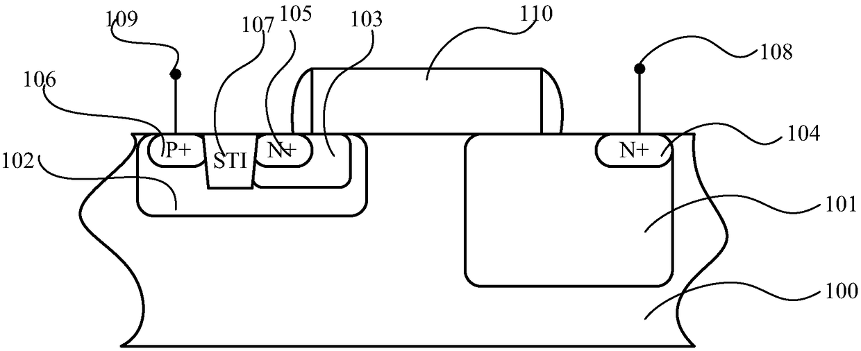
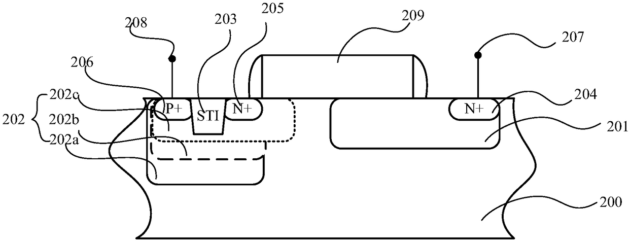
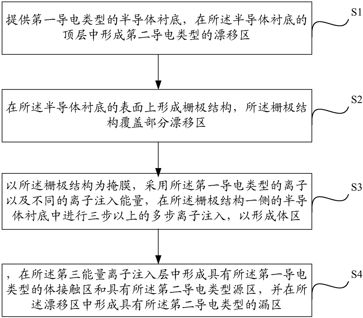
[0040] Please refer to figure 1 , an LDMOS device comprising: a semiconductor substrate 100, a drift region 101 and a deep well 102 arranged in the semiconductor substrate 100, a body region 103 arranged in the deep well 102, a gate arranged on the semiconductor substrate 100 A pole structure 110, a source region 105, a body contact region 106 and a shallow trench isolation structure 107 disposed in the body region 103, and electrodes 108 and 109 drawn from the drain region 104 and the body contact region 106, respectively. The body contact region 106 is used to adjust and control the potential of the body region 103, the doping types of the drift region 101 and the deep well 102 are opposite, and the doping type of the body region 103 and the deep well 102 are the same, thereby increasing the breakdown voltage and reduce the on-resistance. In this typical LDMOS device structure, due to the formation of the drift region 101 and the deep well 102, two deep well implant masks are used as masks, and they are implemented by ion implantation respectively, while the body region 103 needs It is formed by an additional mask and ion implantation, the manufacturing process is relatively complicated, and the manufacturing cost is relatively high.
[0041] One of the core ideas of the technical solution of the present invention is to combine the deep well and the body region of the LDMOS device into one, thereby obtaining a new type of LDMOS device with low on-resistance and high breakdown voltage, so that the manufacturing process can be Compatible with the CMOS process, it can effectively improve the integration level, reduce the production cost and process difficulty, and at the same time avoid the process of using an additional mask to form the body region, saving a mask.
[0042] In order to make the above objects, features and advantages of the present invention more clearly understood, the specific embodiments of the present invention will be described in detail below with reference to the accompanying drawings. Many specific details are set forth in the following description to facilitate a full understanding of the present invention, but the present invention can also be implemented in other ways different from those described herein, and those skilled in the art can do so without departing from the connotation of the present invention. Similar promotion, therefore, the present invention is not limited by the specific embodiments disclosed below. Next, the present invention is described in detail with reference to the schematic diagrams. When describing the embodiments of the present invention in detail, for the convenience of explanation, the cross-sectional views showing the device structure will not be partially enlarged according to the general scale, and the schematic diagrams are only examples, which should not be limited here. The scope of protection of the present invention. In addition, the three-dimensional spatial dimensions of length, width and depth should be included in the actual production.
[0043] Please refer to figure 2 The present invention provides an LDMOS device, comprising: a semiconductor substrate 200, a gate structure 209 located on the surface of the semiconductor substrate 200, and a drift region 201, a body region 202, a drain region 204, Source region 205 , body contact region 206 .
[0044] The semiconductor substrate 200 can be various semiconductor materials well known to those skilled in the semiconductor field, including silicon or silicon germanium (SiGe) of single crystal or polycrystalline structure, and can also be silicon containing doping ions such as N-type or P-type doping Or silicon germanium, which can also include compound semiconductor structures such as silicon carbide, indium antimonide, lead telluride, indium arsenide, indium phosphide, gallium arsenide, gallium antimonide, gallium nitride, aluminum nitride, indium nitride Alloy semiconductors or combinations thereof; may also be silicon-on-insulator (SOI); may also be strained silicon, strained silicon germanium, or other strained materials. The semiconductor substrate may be a blank semiconductor material substrate or a semiconductor substrate on which various semiconductor structures, devices and circuits have been formed. Optionally, the semiconductor substrate 300 is a substrate having a semiconductor epitaxial layer, for example, a substrate having a P-type substrate and a P-type epitaxial layer. Various semiconductor structures, devices and circuits can be formed in the substrate, while the semiconductor epitaxial layer Used to make LDMOS devices.
[0045] The gate structure 209 may include a gate dielectric layer located on the semiconductor substrate 200 between the body region 202 and the drift region 201, a gate electrode (which can be made of polysilicon or metal) located on the gate dielectric layer, and a gate electrode and a gate electrode located on the gate dielectric layer. Side walls for medium side walls. The body region 202 extends laterally toward the drift region 201 , and may be spaced from the drift region 201 , or may be adjacent to the drift region 201 . Both the body region 202 and the drift region 202 have a part of their surface covered by the gate structure 209 , which is used as a channel, and the drain region 204 is provided in the drift region 201 for drawing out the drain electrode 207 . The source region 205 and the body contact region 206 are both disposed in the third ion energy implantation layer 202c of the body region 202, and can be adjacent to each other or separated by a shallow trench isolation structure. In this embodiment, the source region 205 and the body contact region are 206 are separated by shallow trench isolation structures 203 . And the source region 205 and the drain region 204 are located at two ends of the channel, ie, two sides of the gate structure 209 , respectively. The body contact region 206 is located in the body region 202 and on the side of the source region 205 away from the gate structure 209 for drawing out the electrode 208 and adjusting and controlling the potential of the body region 202 to avoid floating body effect. The drift region 201 is used to change the distribution of the electric field in the LDMOS device and increase the breakdown voltage of the LDMOS device. The doping type of the semiconductor substrate 200 , the body region 202 and the body contact region 206 are all of the first conductivity type, the source region 205 , the drain region 204 and the drift region 201 are all of the second conductivity type, and the source region 205 and the drain region 204 are of the second conductivity type. The ion doping concentration is much higher than that of the drift region 201. For example, the doping types of the semiconductor substrate 200, the body region 202, and the body contact region 206 are all P-type, and the source region 205, the drain region 204, and the drift region 201 are all N-type. type, the LDMOS device is an LDNMOS device; for another example, the doping type of the semiconductor substrate 200, the body region 202, and the body contact region 206 are all N-type, and the source region 205, the drain region 204, and the drift region 201 are all P-type, Then the LDMOS device is an LDPMOS device.
[0046] In this embodiment, the body region 202 includes a first energy ion implantation layer 202a, a second energy ion implantation layer 202b and a third energy ion implantation layer 202c which are formed by ion implantation with sequentially decreasing ion implantation energy. The implantation energy is different, so that the depths of the first energy ion implantation layer 202a, the second energy ion implantation layer 202b and the third energy ion implantation layer 202c in the semiconductor substrate 200 are successively shallower, that is, the first energy ion implantation layer 202a is located at the bottom, the second energy ion implantation layer 202b is located above the first energy ion implantation layer 202a, the third energy ion implantation layer 202c is located above the second energy ion implantation layer 202b, the first energy ion implantation layer 202a, the third energy ion implantation layer 202c The width of the second energy ion implantation layer 202b and the third energy ion implantation layer 202c extending laterally to the drift region 201 depends on the ion implantation angle. Therefore, the second energy ion implantation layer 202b can be completely located in the first energy ion implantation layer 202a. The lateral extension of the left side of the second energy ion implantation layer 202b away from the drift region 201 or the lateral extension of the right side toward the drift region 201 may extend beyond the first energy ion implantation layer 202a. Similarly, the third energy ion implantation layer 202c may be completely located in the second energy ion implantation layer 202b. The lateral extension of the ion implantation layer 202b and the third energy ion implantation layer 202c on the left side away from the drift region 201 or the lateral extension of the right side toward the drift region 201 may exceed the second energy ion implantation layer 202b. Therefore, if figure 2 As shown, the first energy ion implantation layer 202a, the second energy ion implantation layer 202b, and the third energy ion implantation layer 202c all extend laterally to the drift region 201 and are spaced apart from the drift region 201, thereby realizing The body region 202 is spaced apart from the drift region 201; and in other embodiments of the present invention, the first energy ion implantation layer 202a, the second energy ion implantation layer 202b and the third energy ion implantation layer 202c are all laterally The ground extends to the drift region 201, and at least one of the layers is adjacent to the drift region 201, so that the body region 202 is adjacent to the drift region 201, for example Figure 4C Among them, the first energy ion implantation layer 402 a , the second energy ion implantation layer 402 b and the third energy ion implantation layer 402 c are all adjacent to the drift region 401 , so that the body region 402 is adjacent to the drift region 401 .
[0047] In this embodiment, the ion implantation energy of the first energy ion implantation layer 202a is 200KeV˜450KeV, the ion implantation energy of the second energy ion implantation layer 202b is 80KeV˜150KeV, and the ion implantation energy of the third energy ion implantation layer 202c The ion implantation energy is 5KeV~50KeV. In addition, the ion implantation dose for forming the third energy ion implantation layer is higher than the ion implantation dose for forming the first energy ion implantation layer and the second energy ion implantation layer, respectively, for example, the first energy ion implantation dose The ion implantation dose of the implanted layer is 1e 13 /cm 2 ~5e 13 /cm 2 , the ion implantation dose of the second energy ion implantation layer is 1e 13 /cm 2 ~5e 13 /cm 2 , the ion implantation dose of the third energy ion implantation layer is 2e 13 /cm 2 ~5e 14 /cm 2.
[0048] In this embodiment, the body contact region 206 and the source region 205 are both located in the third energy ion implantation layer 202c, and the drain region 204 is connected to the first energy ion implantation layer 202a, the second energy ion implantation layer 202b and the third energy ion implantation layer 202b. 202c are all spaced apart to achieve the separation of the source region 205 and the drain region 204.
[0049] The first energy ion implantation layer 202a can compensate for the inversion ions diffused from the drift region 201, the second energy ion implantation layer 202b can adjust the threshold voltage of the LDMOS device, and the third energy ion implantation layer 202c can form a shallow junction or ultra Shallow junction can reduce short channel effect, reduce on-resistance, and prevent punch through. Therefore, the gate structure 209 needs to cover at least a part of the third energy ion implantation layer 202c of the body region 202 . In this embodiment, the gate structure 209 covers the first energy ion implantation layer 202a and the second energy ion implantation layer of the body region 202 respectively. layer 202b and a part of the third energy ion implantation layer 202c; in other embodiments of the present invention, the gate structure 209 may cover only a part of the first energy ion implantation layer 202a and the third energy ion implantation layer 202c of the body region 202 , without covering the second energy ion implantation layer 202b at all, or only covering a part of the third energy ion implantation layer 202c and the second energy ion implantation layer 202b in the body region 202, but not covering the first energy ion implantation layer 202a at all .
[0050] From the above, the first energy ion implantation layer 202a, the second energy ion implantation layer 202b and the third energy ion implantation layer 202c can make the body region 202 of the present invention equivalent to the deep well and the deep well in the prior art. The body region, that is, the deep well in the prior art and the body region in the deep well are combined into one, and the distribution of doping ions is more reasonable, thereby reducing the on-resistance and increasing the breakdown voltage.
[0051] Optionally, the depth of the body region 202 is relatively deep, and the depth of the drift region 201 is relatively shallow, so as to improve the withstand voltage capability of the device, that is, at least the first energy ion implantation layer 202a in the body region 202 extends downward in the semiconductor substrate 200 . is deeper than the depth to which the drift region 201 extends downward in the semiconductor substrate 200 .
[0052] Optionally, the doping concentration of each ion implantation layer in the body region 202 is greater than the doping concentration of the drift region 201, so as to increase the breakdown voltage and reduce the on-resistance.
[0053] The present invention also provides a method for manufacturing the above-mentioned LDMOS device, comprising the following steps:
[0054]S1, providing a semiconductor substrate of the first conductivity type, and forming a drift region of the second conductivity type in the top layer of the semiconductor substrate;
[0055] S2, forming a gate structure on the surface of the semiconductor substrate, the gate structure covering part of the drift region;
[0056] S3, using the gate structure as a mask, using the ions of the first conductivity type and different ion implantation energies to perform three or more multi-step ion implantation in the semiconductor substrate on one side of the gate structure , to form a body region, the body region and the drift region are located on both sides of the gate structure, including a first energy in which the ion implantation energy is successively reduced and the depth extending downward in the semiconductor substrate is successively shallower an ion implantation layer, a second energy ion implantation layer and a third energy ion implantation layer, and the first energy ion implantation layer, the second energy ion implantation layer and the third energy ion implantation layer extend laterally to the drift region, and is spaced apart from or adjacent to the drift region;
[0057] S4, forming a body contact region with the first conductivity type and a source region with the second conductivity type in the third energy ion implantation layer, and forming a body contact region with the second conductivity type in the drift region The drain region is spaced apart from the first energy ion implantation layer, the second energy ion implantation layer and the third energy ion implantation layer.
[0058] Please refer to Figure 4A , in step S1, firstly, the provided semiconductor substrate 400 may be various semiconductor materials well known to those skilled in the semiconductor field, including silicon or silicon germanium (SiGe) of single crystal or polycrystalline structure, and may also contain dopant ions For example N-type or P-type doped silicon or silicon germanium, may also include compound semiconductor structures such as silicon carbide, indium antimonide, lead telluride, indium arsenide, indium phosphide, gallium arsenide, gallium antimonide, nitrogen Gallium nitride, aluminum nitride, indium nitride alloy semiconductors or combinations thereof; also silicon-on-insulator (SOI); also strained silicon, strained silicon germanium, or other strained materials. The semiconductor substrate may be a blank (ie, no structure is formed, only low doping) semiconductor material substrate, or a semiconductor substrate on which various semiconductor structures, devices and lines have been formed. Optionally, the semiconductor substrate 300 is a substrate having a semiconductor epitaxial layer, for example, a substrate having a P-type substrate and a P-type epitaxial layer. Various semiconductor structures, devices and circuits can be formed in the substrate, while the semiconductor epitaxial layer Used to make LDMOS devices. Then, a photolithography process and an ion implantation process are used to form a drift region 401 in the semiconductor substrate 400. The conductivity type (ie, the doping type) of the drift region 401 is opposite to that of the semiconductor substrate 400, that is, the semiconductor substrate 400 is of the first conductivity type. , then the drift region 401 is of the second conductivity type, and the drift region 401 is a low-doped region relative to the source and drain regions formed later. Specifically, the surface of the semiconductor substrate 400 is first coated with photoresist, which can utilize the depth of the CMOS process. The well implant mask and the photolithography process form the drift region pattern (ie the deep well region pattern) in the photoresist, thereby opening the region of the semiconductor substrate 400 where the drift region 401 is to be formed (ie the drift region ion implantation window), Then, the low-doped ion implantation with the opposite doping type of the semiconductor substrate 400 is performed on the semiconductor substrate region where the drift region 401 is to be formed, and the ion implantation direction is perpendicular to the surface of the semiconductor substrate 400. The ions diffuse into place in the top surface of the semiconductor substrate 400, forming a drift region; the photoresist is then removed. The ion implantation energy and ion implantation dose (ie doping concentration) used for forming the drift region may be the same as those in the prior art, for example, the ion implantation dose may be 1e 12 /cm 2 ~6e 12 /cm 2 within the range. When the semiconductor substrate 400 is P-type, phosphorus and/or arsenic ion implantation is employed as the ion implantation of the N-type drift region. Further, the drift region 401 can also be performed in multiple steps, each step using different implantation energy and implantation dose, thereby improving the performance of the drift region 401 . It should be noted that the lateral extension width of the drift region 401 in the semiconductor substrate 400 may occupy the entire top layer of the semiconductor substrate 400 (ie, the entire active region) or may occupy part of the top layer of the semiconductor substrate 400 ( i.e. formed in part of the active region). Figure 4A The drift region 401 is shown throughout the top layer of the semiconductor substrate 400 .
[0059] Please continue to refer to Figure 4A In step S2, a gate structure 409 is formed on the surface of the semiconductor substrate 400 through a gate formation process. The specific formation process includes: firstly forming a gate dielectric layer and a gate layer on the surface of the semiconductor substrate 400 in sequence, Wherein, the material of the gate dielectric layer can be an oxide layer, the material of the corresponding gate layer can be polysilicon, the material of the gate dielectric layer can also be a high-K dielectric layer, and the material of the corresponding gate layer can be metal; then use CMOS In the gate plate in the process, the gate layer and the gate dielectric layer are lithography and etched to form a gate; then, a spacer material is deposited on the gate surface and the surface of the semiconductor substrate 400, and the spacer is etched In the process, spacers are formed on the sidewalls of the gate, thereby obtaining the gate structure 409 . Wherein, when the drift region 401 formed in the top layer of the semiconductor substrate 400 occupies the entire top layer of the semiconductor substrate 400, the gate structure 409 is actually formed on the surface of the drift region 401, and the drift on the side of the gate structure 409 The drift region 401 remains, while the drift region 401 on the other side will be used to form the body region; when the drift region formed in the top layer of the semiconductor substrate 400 occupies part of the top layer of the semiconductor substrate 400, the drift region 401 is located on one side of the gate structure 409 and one end is covered by the gate structure 409 , and the other side of the gate structure is the semiconductor substrate 400 without the drift region 401 formed, which is used to form the body region.
[0060] Please refer to Figure 4B , in step S3, first coat the photoresist on the surface of the semiconductor substrate 400 and the gate structure 409, and then expose and develop the photoresist on the side of the gate structure 409 to expose part of the semiconductor The surface of the substrate 400 is used as the ion implantation window of the body region 402, and the ion implantation window and the pre-reserved drift region 401 are separated on both sides of the gate structure 409; then the gate structure 409 and the remaining photoresist are used as masks film, using different ion implantation energies to perform three or more multi-step ion implantation on the surface of the semiconductor substrate 400 in the ion implantation window to form a body region 402. The conductivity type (ie doping type) of the body region 402 is different from that of the semiconductor. The substrate 400 is the same, that is, the semiconductor substrate 400 is of the first conductivity type, the body region 402 is also of the first conductivity type, and the body region 402 is also a low-doped region relative to the source and drain regions formed subsequently. In this embodiment, since the drift region 401 formed in step S1 is covered with the top layer of the semiconductor substrate 400, the multi-step ion implantation is actually performed in the drift region on the side of the gate structure 409, thereby forming The body region 402 adjacent to the remaining drift region 401 . In other embodiments of the present invention, when the drift region 401 formed in the top layer of the semiconductor substrate 400 only occupies part of the top layer, that is, the drift region 401 is located on one side of the gate structure 409 and One end is covered by the gate structure 409, and the formed ion implantation window and the drift region 401 are separated on both sides of the gate structure 409. At this time, the multi-step ion implantation is performed when the gate structure 409 is far from the gate structure 409. in the semiconductor substrate 400 on one side of the drift region 401, thereby forming a body region 402 adjacent to or spaced apart from the drift region 401 (eg figure 2 shown). In this embodiment, the ion implantation energy and ion implantation dose of each ion implantation of the multi-step ion implantation are different. For example, the ion implantation energy of each step of ion implantation decreases sequentially, and the annealing process is used to make the implanted ions in the Diffusion into place in the top surface of the semiconductor substrate 400 , thereby forming a first energy ion implantation layer 402 a and a second energy ion implantation layer 402 b in which the ion implantation energy is successively reduced and the depth extending downward in the semiconductor substrate 400 is successively shallower and the third energy ion implantation layer 402, specifically, when the conductivity type of the semiconductor substrate 400 is P-type, in the ion implantation window, firstly, an ion implantation energy of 200KeV˜450KeV, 1e 13 /cm 2 ~5e 13 /cm 2 The injected boron (B) ions are vertically implanted to form the first energy ion implantation layer 402a to compensate for the inversion ions diffused from the drift region 401; 13 /cm 2 ~5e 13 /cm 2 The injected boron fluoride (B) ions are vertically implanted to form the second energy ion implantation layer 402b to adjust the threshold voltage of the LDMOS device and form the channel; 2e 13 /cm 2 ~5e 14 /cm 2 The injected phosphorus (P) ions are implanted at a large angle, and the angle α between the ion implantation direction and the surface of the semiconductor layer substrate is 30°-45°, which is used to form the third energy ion implantation layer 402c to form channel, and use shallow junction or ultra-shallow junction to reduce short channel effect, reduce on-resistance, and prevent punch through effect. In addition, the third energy ion implantation layer 402c is formed laterally to the drift region 401 Extending and adjoining the drift region 401, the electric field distribution of the channel region can be optimized, the on-resistance can be reduced, and the breakdown voltage can be improved.
[0061] Step S3 uses the gate structure as a mask, and forms the body region 402 through multi-step ion implantation with different implantation energies, instead of using two implantation masks (for example, P well implantation mask + P body region in the prior art) On the one hand, it saves the mask, and at the same time is compatible with the CMOS process, reducing the production cost and process difficulty; on the other hand, it optimizes the source region 405 side formed subsequently. and the electric field distribution of the channel region under the gate structure 409, thereby reducing the on-resistance and increasing the breakdown voltage.
[0062] The annealing process in step S3 is mainly for repairing lattice defects after ion implantation, activating impurity ions, and reducing on-resistance. Therefore, after all ion implantation in the multi-step ion implantation, only one annealing process may be performed, and also An annealing process may be performed after each step of the multi-step ion implantation.
[0063] Please refer to Figure 4C , in step S4, using the source-drain region implantation mask in the CMOS process, and using the gate structure 409 as a mask, heavily doped ion implantation (ie, ion implantation with low implantation energy and high implantation dose) is performed to A drain region 404 is formed in the drift region 401, and a source region 405 and a body contact region 406 are formed in the third energy ion implantation layer 402c of the body region 402, wherein the body contact region 406 is located beside the source region 405, The source region 405 and the body contact region 406 are separated from the drain region 404 by the gate structure 409, that is, the body contact region 406 and The source region 405 is located on one side of the gate structure 409, the drain region 404 is located on the other side of the gate structure 409, and is connected to the first energy ion implantation layer 402a, the second energy ion implantation layer 402b and the third energy ion implantation layer 402b. The ion implantation layers 402c are each spaced apart. The source region 405 and the drain region 404 are of the same conductivity type as the drift region 401 , and the body contact region 406 is of the same conductivity type as the body region and the semiconductor substrate 400 . Please refer to Figure 4C , when the conductivity type of the semiconductor substrate 400 is P-type, the conductivity types of the source region 405 and the drain region 404 are both N-type, and the body contact region 406 is P-type. In other embodiments of the present invention, the body contact region 406 , the source region 405 and the drain region 404 may also be formed through a diffusion doping process.
[0064] Additionally, the body contact region 406 may be adjacent to the source region 405 (eg Figure 4C shown), can also be spaced apart from the source region 405 (eg figure 2The middle body contact region 206 is separated from the source region 205 by a shallow trench isolation structure STI 203). When the body contact region 406 is spaced apart from the source region 405 , the trench isolation structure may be fabricated by shallow trench isolation (STI) technology before the body contact region 406 and the source region 405 are formed in the body region 402 . The photolithography and etching process etch away part of the semiconductor substrate material including the body region 402 to form a shallow trench, and then fill the shallow trench with oxide isolation material to form the isolation body contact region 406 and the source region 405 shallow trench isolation structure.
[0065] After step S4, a metal silicide, such as titanium or cobalt silicide, can be formed on the surface of the body contact region 406 and the drain region 404 by a self-aligned silicide process, and then the electrodes 407 and 408 are drawn out to reduce the contact resistance. .
[0066] To sum up, the LDMOS device and its manufacturing method of the present invention, on the one hand, can be compatible with the CMOS process, can effectively improve the integration, reduce the production cost and process difficulty; on the other hand, the gate structure is used as a mask, and the Multi-step ion implantation with different ion implantation energies forms a body region with a first energy ion implantation layer, a second energy ion implantation layer and a third energy ion implantation layer with successively shallower depths, which is equivalent to changing the existing deep trap. It is combined with the body region, thereby avoiding the process of forming the body region by means of an additional mask, saving the mask, and finally producing an LDMOS device with low on-resistance and high breakdown voltage.
[0067] Obviously, those skilled in the art can make various changes and modifications to the invention without departing from the spirit and scope of the invention. Thus, provided that these modifications and variations of the present invention fall within the scope of the claims of the present invention and their equivalents, the present invention is also intended to include these modifications and variations.

PUM

no PUM

Description & Claims & Application Information

We can also present the details of the Description, Claims and Application information to help users get a comprehensive understanding of the technical details of the patent, such as background art, summary of invention, brief description of drawings, description of embodiments, and other original content. On the other hand, users can also determine the specific scope of protection of the technology through the list of claims; as well as understand the changes in the life cycle of the technology with the presentation of the patent timeline. Login to view more.

Similar technology patents

Central controller of vehicle-mounted broadcasting equipment

InactiveCN104113385AShort switching timesLower on-resistanceBroadcast specific applicationsBroadcast systems controlIn vehicleData transmission
Owner:SUZHOU HUAQI INTELLIGENT TECH

Classification and recommendation of technical efficacy words

  • Improve breakdown voltage
  • Lower on-resistance

Carrier-storing grooved gate IGBT with P-type floating layer

InactiveCN101694850AReduce forward voltage dropImprove breakdown voltageSemiconductor devicesJFETHigh concentration
Owner:UNIV OF ELECTRONIC SCI & TECH OF CHINA

High-Frequency Power MESFET Buck Switching Power Supply

Owner:ADVANCED ANALOGIC TECHNOLOGIES INCORPORATED

Semiconductor device

InactiveUS20090189191A1Improved breakdown voltage characteristicsLower on-resistanceTransistorSolid-state devicesField-effect transistorCathode electrode
Owner:FURUKAWA ELECTRIC CO LTD
Why Eureka
Try Eureka