
Vertical power diode with gradient-constituent drift-layers and fabrication method of vertical power diode

A technology of power diodes and drift layers, which is applied in the field of microelectronics, can solve the problems of device on-resistance and output current deterioration, uneven distribution of device electric field strength, and weaken the electric field strength of the drift layer, so as to avoid output current reduction and reverse The effect of effectively increasing the breakdown voltage and avoiding the increase of on-resistance

Active Publication Date: 2018-09-28
XIDIAN UNIV
View PDF5 Cites 1 Cited by
  • Summary
  • Abstract
  • Description
  • Claims
  • Application Information

AI Technical Summary

Problems solved by technology

[0005] After years of theoretical and experimental research, the researchers found that the above-mentioned traditional GaN-based vertical power diode structure has inherent defects, which will lead to extremely uneven electric field intensity distribution in the device, and there is a very high electric field peak near the anode in the upper part of the drift layer. , and the closer to the cathode in the drift layer, the smaller the electric field, causing premature breakdown of the device
In addition, in the traditional GaN-based vertical power diode, even if the field plate technology is used, the electric field intensity near the anode in the drift layer is only weakened to a certain extent, while the electric field distribution in other regions in the drift layer is not improved.
Therefore, the drift layer of traditional GaN-based vertical power diodes does not actually fully play the role of carrying the reverse withstand voltage, resulting in the breakdown voltage of the device is often much lower than the theoretical expected value
Although the breakdown voltage of GaN-based vertical power diodes can be improved to a certain extent by reducing the doping concentration of the drift layer, the on-resistance and output current of the device will deteriorate.
Therefore, in traditional GaN-based vertical power diodes, there is a very prominent contradiction between the breakdown voltage and on-resistance of the device

Method used


Image

  • Vertical power diode with gradient-constituent drift-layers and fabrication method of vertical power diode
  • Vertical power diode with gradient-constituent drift-layers and fabrication method of vertical power diode
  • Vertical power diode with gradient-constituent drift-layers and fabrication method of vertical power diode

Examples


Embodiment 1

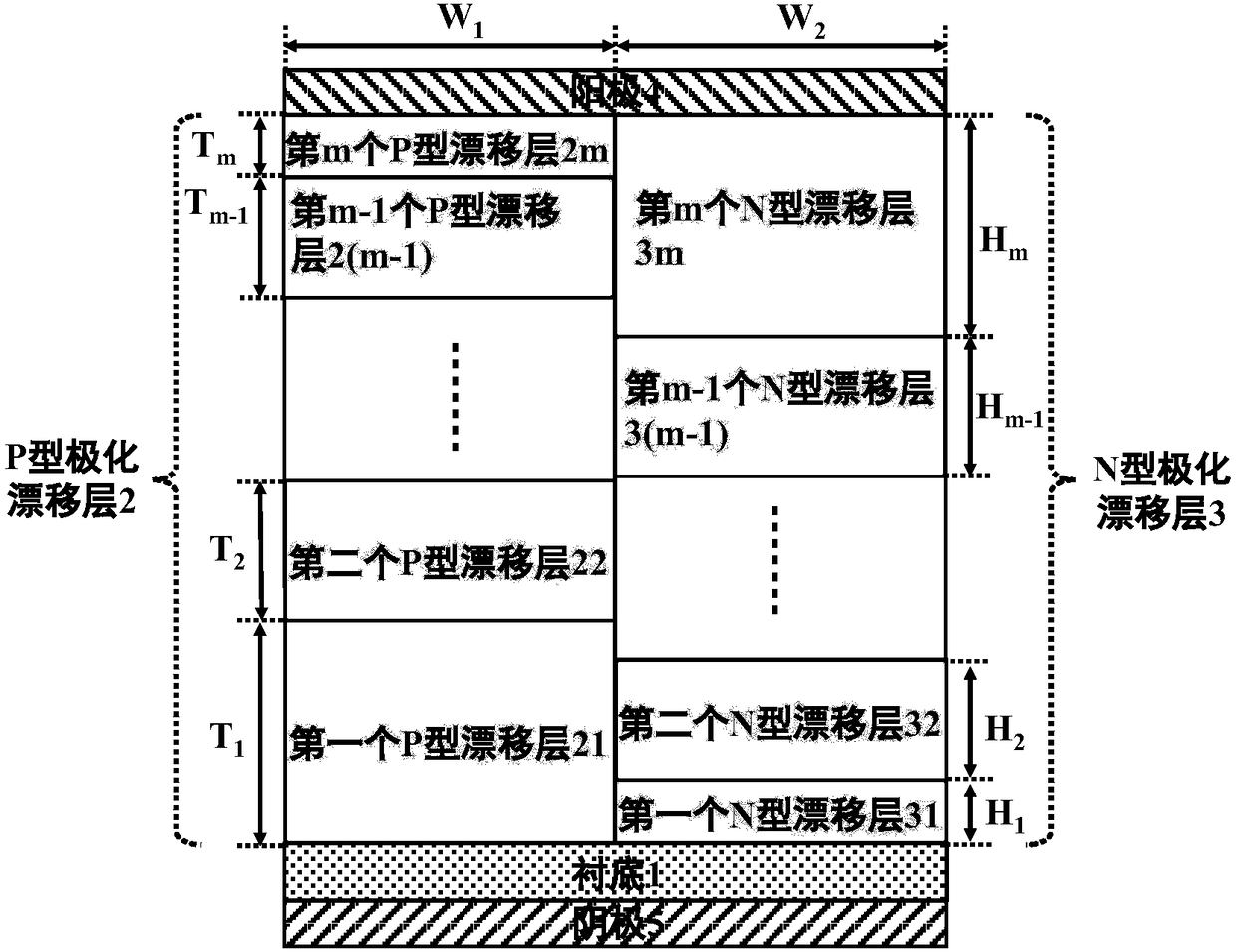
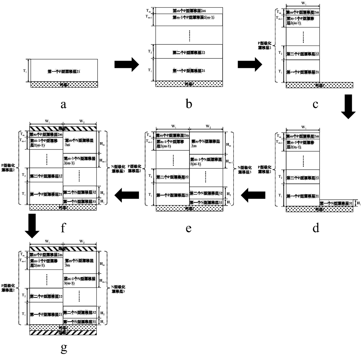
[0062] Embodiment 1: Manufacturing a drift layer vertical power diode with a gradient composition drift layer whose layer number m is 1.

[0063] Step 1. Fabricate a P-type polarization drift layer.

[0064] 1.1) Make the first layer of P-type drift layer, such as image 3 a.

[0065] in the use of n + AlGaN semiconductor material is epitaxially grown on a GaN substrate using metal-organic chemical vapor deposition to form a thickness T 1The first layer of P-type drift layer is 1.0 μm, the Al composition of the lower surface is 0, and the Al composition of the upper surface is 0.15, and the Al composition increases linearly from the lower surface to the upper surface of the layer;

[0066] The process conditions of metal-organic chemical vapor deposition technology are as follows: temperature is 980°C, pressure is 45Torr, flow rate of hydrogen gas is 4400 sccm, flow rate of ammonia gas is 4400 sccm, flow rate of gallium source is 35 μmol / min, flow rate of aluminum source in...

Embodiment 2

[0079] Embodiment 2: Fabricate a drift layer vertical type power diode with a gradient composition drift layer whose number m is 2.

[0080] Step 1. Fabricate a P-type polarization drift layer.

[0081] 1a) Make the first layer of P-type drift layer, such as image 3 a.

[0082] in the use of n + AlGaN semiconductor material is epitaxially grown on a substrate of GaN-type GaN using metal-organic chemical vapor deposition technology to form a thickness T 1 The first P-type drift layer is 1.0 μm, the Al composition of the lower surface is 0, and the Al composition of the upper surface is 0.1, and the Al composition increases linearly from the lower surface to the upper surface of the layer;

[0083] The process conditions of metal-organic chemical vapor deposition technology are as follows: temperature is 980°C, pressure is 45Torr, flow rate of hydrogen gas is 4000 sccm, flow rate of ammonia gas is 4000 sccm, flow rate of gallium source is 35 μmol / min, flow rate of aluminum s...

Embodiment 3

[0101] Embodiment 3: Fabricate a drift layer vertical type power diode with a gradient composition drift layer whose number m is 3.

[0102] Step A. Fabricate a P-type polarization drift layer.

[0103] A1) Make the first layer of P-type drift layer, such as image 3 a.

[0104] in the use of n + Metal-organic chemical vapor deposition technology was used on the substrate of GaN-type GaN at a temperature of 980°C, a pressure of 40 Torr, a flow rate of hydrogen gas of 3800 sccm, a flow rate of ammonia gas of 3800 sccm, a flow rate of gallium source of 30 μmol / min, and a flow rate of aluminum source of 5 μmol / min. Under the process conditions of linearly increasing to 7mol / min, the epitaxial AlGaN semiconductor material is formed to form a thickness T 1 The first P-type drift layer is 2.0 μm, the Al composition of the lower surface is 0, and the Al composition of the upper surface is 0.1, and the Al composition increases linearly from the lower surface to the upper surface of...


PUM

PropertyMeasurementUnit
Thicknessaaaaaaaaaa
Thicknessaaaaaaaaaa
Widthaaaaaaaaaa

Abstract

The invention discloses a vertical power diode with gradient-constituent drift-layers, and mainly solves the problem that high breakdown voltage and low conduction resistance of a traditional verticalpower device cannot be simultaneously achieved. The gradient-constituent drift-layer vertical power diode comprises a substrate (1), a P-type polarization drift layer (2) and an N-type polarization drift layer (3), wherein a positive electrode (4) is deposited on the P-type polarization drift layer (2) and the N-type polarization drift layer (3), a negative electrode (5) is deposited at a lower part of the substrate, the P-type polarization drift layer comprises m layers of AlGaN semiconductor materials of which Al constituents are linearly increased from bottom to top, the P-type polarization drift layer is arranged at a left side of an upper part of the substrate, the N-type polarization drift layer comprises m layers of AlGaN semiconductor layers of which Al constituents are linearly reduced from bottom to top, and the N-type polarization drift layer is arranged at a right side of the upper part of the substrate. By the vertical power diode, high breakdown voltage and low conduction resistance can be simultaneously achieved, and the vertical power diode can be used for a power electronic system.

Description

technical field [0001] The invention belongs to the technical field of microelectronics, in particular to a vertical power diode, which can be used in power electronic systems. technical background [0002] At present, the world's energy and environmental problems have become increasingly prominent, and have become an important obstacle restricting the sustainable development of mankind. The research and development of high-performance, low-loss power semiconductor devices is one of the effective ways to improve the utilization rate of electric energy, save energy, and alleviate the energy crisis. With the development of microelectronics technology, the performance of traditional first-generation Si semiconductor and second-generation GaAs semiconductor power devices is close to the theoretical limit determined by the material itself, and the wide bandgap semiconductor material represented by GaN has a larger forbidden Band width, higher critical breakdown electric field an...

Claims


Application Information

Patent Timeline
IPC IPC(8): H01L29/06H01L29/861H01L21/329
CPCH01L29/0634H01L29/0684H01L29/66121H01L29/8613H01L29/2003H01L29/205H01L29/66212H01L29/872
Inventor 毛维丛冠宇彭紫玲张进成郝跃
Owner XIDIAN UNIV
Features
  • Generate Ideas
  • Intellectual Property
  • Life Sciences
  • Materials
  • Tech Scout
  • Unparalleled Data Quality
  • Higher Quality Content
  • 60% Fewer Hallucinations
Learn More