A kind of ultraviolet detector and its manufacturing method
A technology of ultraviolet detector and manufacturing method, which is applied in the field of ultraviolet detection, can solve the problems that it cannot be used as an ultraviolet detector, and achieve the effects of improving sensitivity, increasing width, and increasing concentration
- Summary
- Abstract
- Description
- Claims
- Application Information
AI Technical Summary
Problems solved by technology
Method used
Image
Examples
Embodiment 1
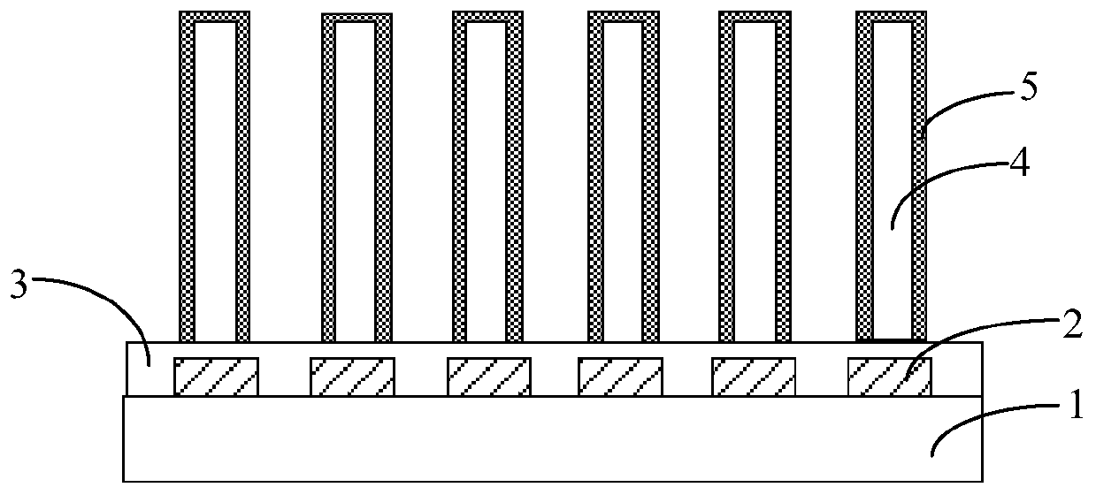
[0057] In order to obtain an ultraviolet detector with higher performance, the present invention provides an ultraviolet detector structure, which mainly includes:
[0058] Substrate;
[0059] The first ohmic contact electrode, formed on the substrate, includes a bottom ohmic contact electrode layer, and several raised structures disposed on the bottom ohmic contact electrode layer;
[0060] The stacked n-type ZnO layer, i-type ZnO layer and p-type ZnO layer are arranged on the surface of the bottom ohmic contact electrode layer and the surface of the raised structure, wherein the i-type ZnO layer is located on the n between the p-type ZnO layer and the p-type ZnO layer;
[0061] The second ohmic contact electrode is formed on a partial surface of the stacked n-type ZnO layer, i-type ZnO layer, and p-type ZnO layer.
[0062] The first ohmic contact electrode in the ultraviolet detector of the present invention is formed on the substrate, including a bottom ohmic contact elec...
Embodiment 2
[0102] The present invention also provides a method for manufacturing the ultraviolet detector in the foregoing embodiment one, such as Figure 5 As shown, it mainly includes the following steps:
[0103] Step S1, providing a substrate;
[0104] Step S2, forming a first ohmic contact electrode on the substrate, wherein the first ohmic contact electrode includes a bottom ohmic contact electrode layer, and several protrusion structures arranged on the bottom ohmic contact electrode layer ;
[0105] Step S3, forming a stack of n-type ZnO layer, i-type ZnO layer and p-type ZnO layer to cover the surface of the bottom ohmic contact electrode layer and the surface of the raised structure, wherein the i-type ZnO layer is located Between the n-type ZnO layer and the p-type ZnO layer;
[0106] Step S4, forming a second ohmic contact electrode to cover part of the top surfaces of the stacked n-type ZnO layer, i-type ZnO layer and p-type ZnO layer.
[0107] Below, refer to Fig. Fig...
PUM
| Property | Measurement | Unit |
|---|---|---|
| height | aaaaa | aaaaa |
| thickness | aaaaa | aaaaa |
| thickness | aaaaa | aaaaa |
Abstract
Description
Claims
Application Information


