Semiconductor device

A semiconductor and device technology, applied in the field of semiconductor integrated circuits, can solve problems such as gate oxide layer breakdown, hot carrier injection, and reliability of high-voltage components, and achieve the effects of increasing depletion, improving reliability, and simple structure

Inactive Publication Date: 2018-10-09
SHANGHAI HUALI INTEGRATED CIRCUTE MFG CO LTD
View PDF3 Cites 7 Cited by
  • Summary
  • Abstract
  • Description
  • Claims
  • Application Information

AI Technical Summary

Problems solved by technology

When high-voltage components are operated at high voltages such as 3.3, 5V or 8V, especially when they reach the saturation range, the electric field strength will deeply affect the reliability of high-voltage components, such as breakdown of the gate oxide layer, hot carrier injection and other problems are prone to occur

Method used


Image

  • Semiconductor device
  • Semiconductor device

Examples


no. 1 example

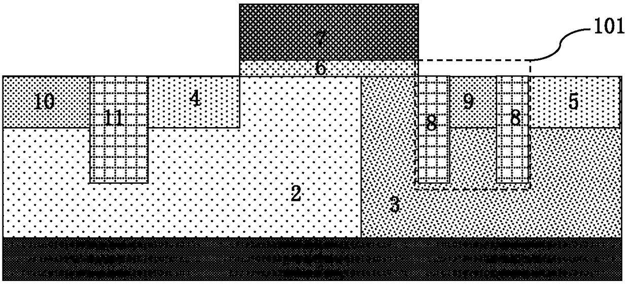
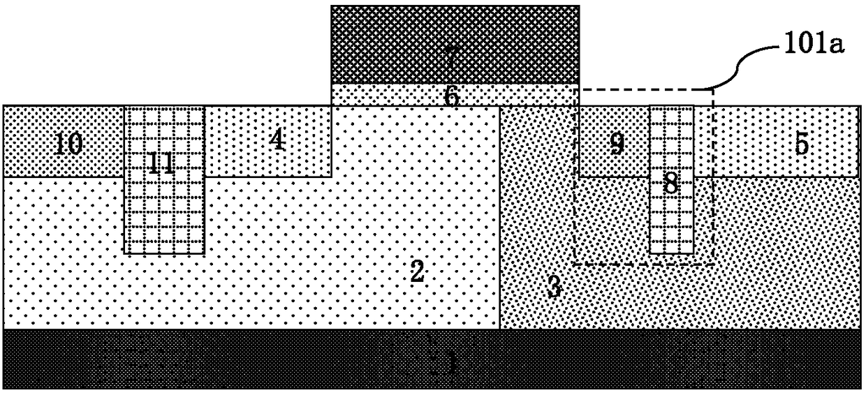
[0036] Such as figure 1 Shown is a structural diagram of the semiconductor device of the first embodiment of the present invention, the semiconductor device of the first embodiment of the present invention includes:

[0037] The channel region 2 is doped with the second conductivity type and the drift region 3 is doped with the first conductivity type.

[0038] The channel region 2 is in lateral contact with the drift region 3 .

[0039] A gate structure formed by stacking a gate dielectric layer 6 and a polysilicon gate 7, the gate structure covers the surface of the channel region 2 and extends to the surface of the drift region 3, and is covered by the gate structure The surface of the channel region 2 is used to form a channel. Preferably, the gate dielectric layer 6 is a gate oxide layer.

[0040] The heavily doped source region 4 of the first conductivity type is formed on the surface of the channel region 2 and self-aligned with the gate structure for the first time....


PUM


Abstract

The invention discloses a semiconductor device. The semiconductor device comprises a channel region, a drift region, a gate structure formed by overlapping a gate dielectric layer and a polysilicon gate, a source region and a drain region, wherein the drain region and a second side of the gate structure are separated by a distance; a drain terminal combination structure formed by more than one first doped region opposite to drain region doping and more than one first shallow trench field oxide is formed between the drain region and a second side of the gate structure; the top of the drain region is connected to a drain electrode formed by a front metal layer through a contact hole, and the first doped region is floated; when the semiconductor device works, through the drain terminal combination structure, the depletion of the drift region is increased and the electric field intensity of the drift region is reduced, and the reliability of the device is improved. According to the device,the reliability of the device can be improved, the characteristics of the native device cannot be influenced, the process cost is not increased, and a selection is provided for high-voltage application.

Description

technical field [0001] The invention relates to a semiconductor integrated circuit, in particular to a semiconductor device. Background technique [0002] In a semiconductor integrated circuit, various devices need to be integrated on the same semiconductor substrate such as a silicon substrate at the same time. A semiconductor integrated circuit usually includes a core circuit (Core) and an input and output (IO) circuit. Each device of the core circuit corresponds to As for the core device, each device of the IO circuit corresponds to the IO device. For the memory, the core circuit corresponds to a storage array composed of storage units, and the stored information of the storage units needs to be operated through the IO circuit. [0003] In addition to core circuits and input and output circuits, it is often necessary to integrate high-voltage devices or high-voltage components with operating voltages and breakdown voltages that are much higher than core devices and IO dev...

Claims


Application Information

Patent Timeline
Patent Type & Authority Applications(China)
IPC IPC(8): H01L29/06H01L29/08
CPCH01L29/0607H01L29/0684H01L29/08H01L29/7835H01L29/0653H01L29/0619
Inventor 王世铭黄志森胡展源
Owner SHANGHAI HUALI INTEGRATED CIRCUTE MFG CO LTD
Why Eureka
Try Eureka