Wafer manufacturing device of solar battery

A technology for solar cells and manufacturing devices, which is applied in the fields of final product manufacturing, sustainable manufacturing/processing, semiconductor/solid-state device manufacturing, etc. It can solve problems such as wafer quality degradation, waste of processing materials, and uneven wafer density. The effect of uniform density and high processing efficiency

Active Publication Date: 2018-10-12
厦门市信邦威科技有限公司
View PDF2 Cites 0 Cited by
  • Summary
  • Abstract
  • Description
  • Claims
  • Application Information

AI Technical Summary

Problems solved by technology

This technical solution realizes extrusion molding of the wafer and increases the density of the wafer, but this technical solution will roll the material on the upper surface of the wafer to one side, resulting in uneven density of the processed wafer, which directly leads to The quality is reduced; there are wafers spilling residue on the edge of the mold cavity, which wastes processing materials; the wafer is rolled intermittently, and the rolling efficiency is not high

Method used


Image

  • Wafer manufacturing device of solar battery
  • Wafer manufacturing device of solar battery
  • Wafer manufacturing device of solar battery

Examples


Embodiment Construction

[0021] In order to make the technical means, creative features, goals and effects achieved by the present invention easy to understand, the present invention will be further described below in conjunction with specific embodiments.

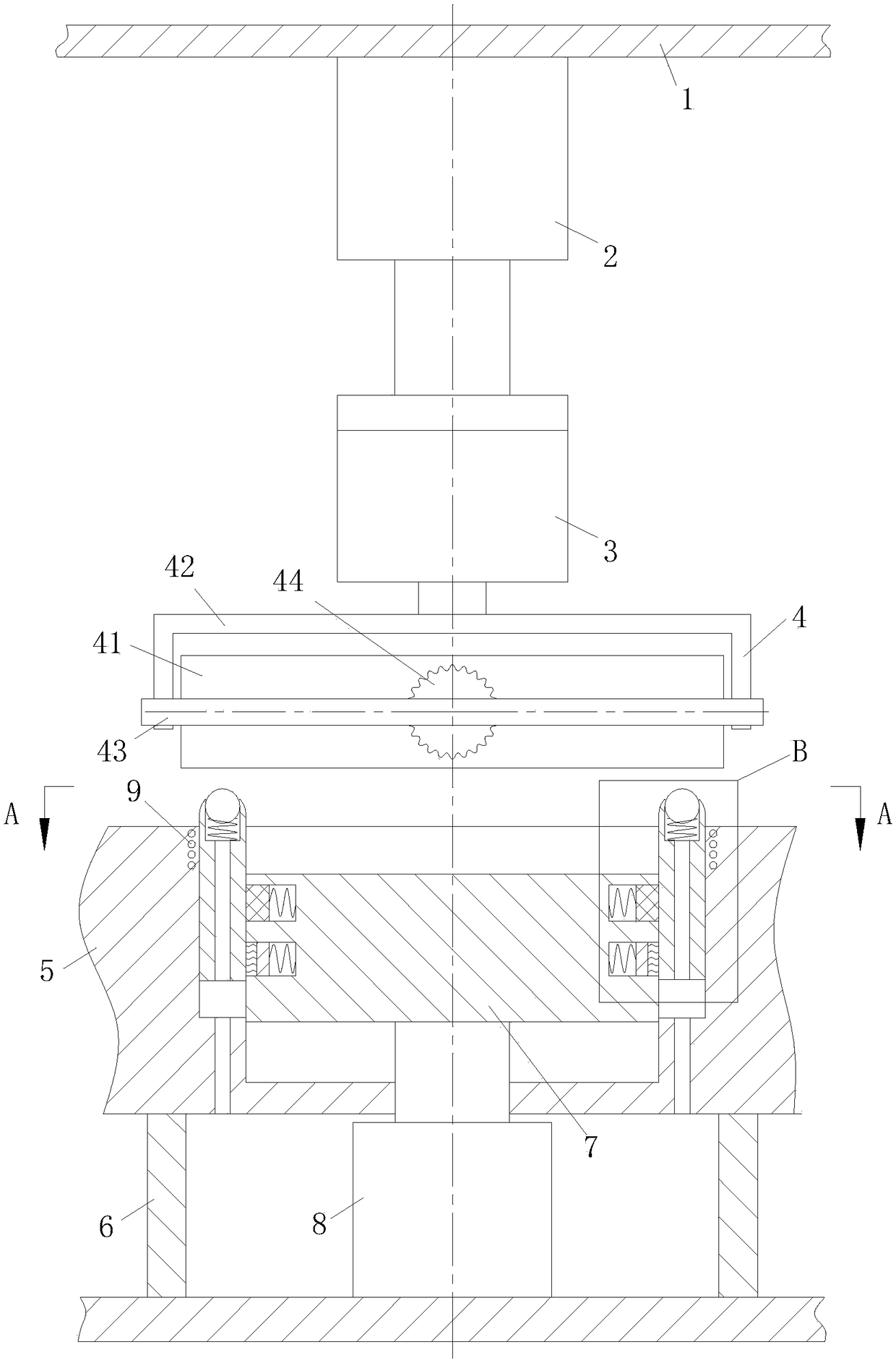
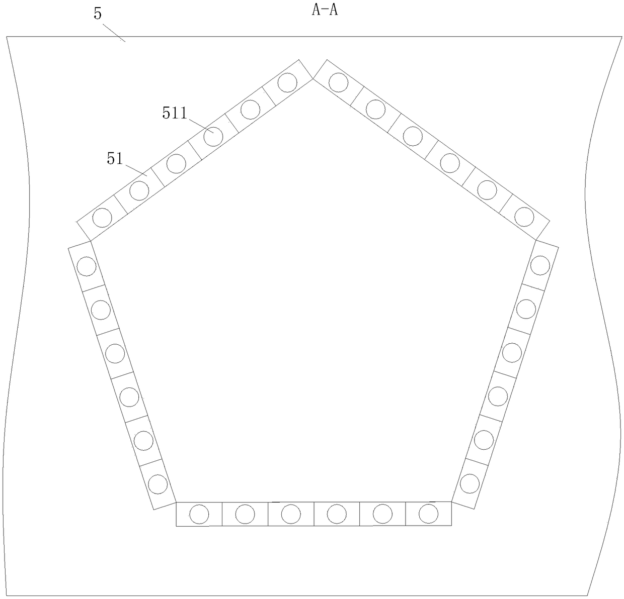
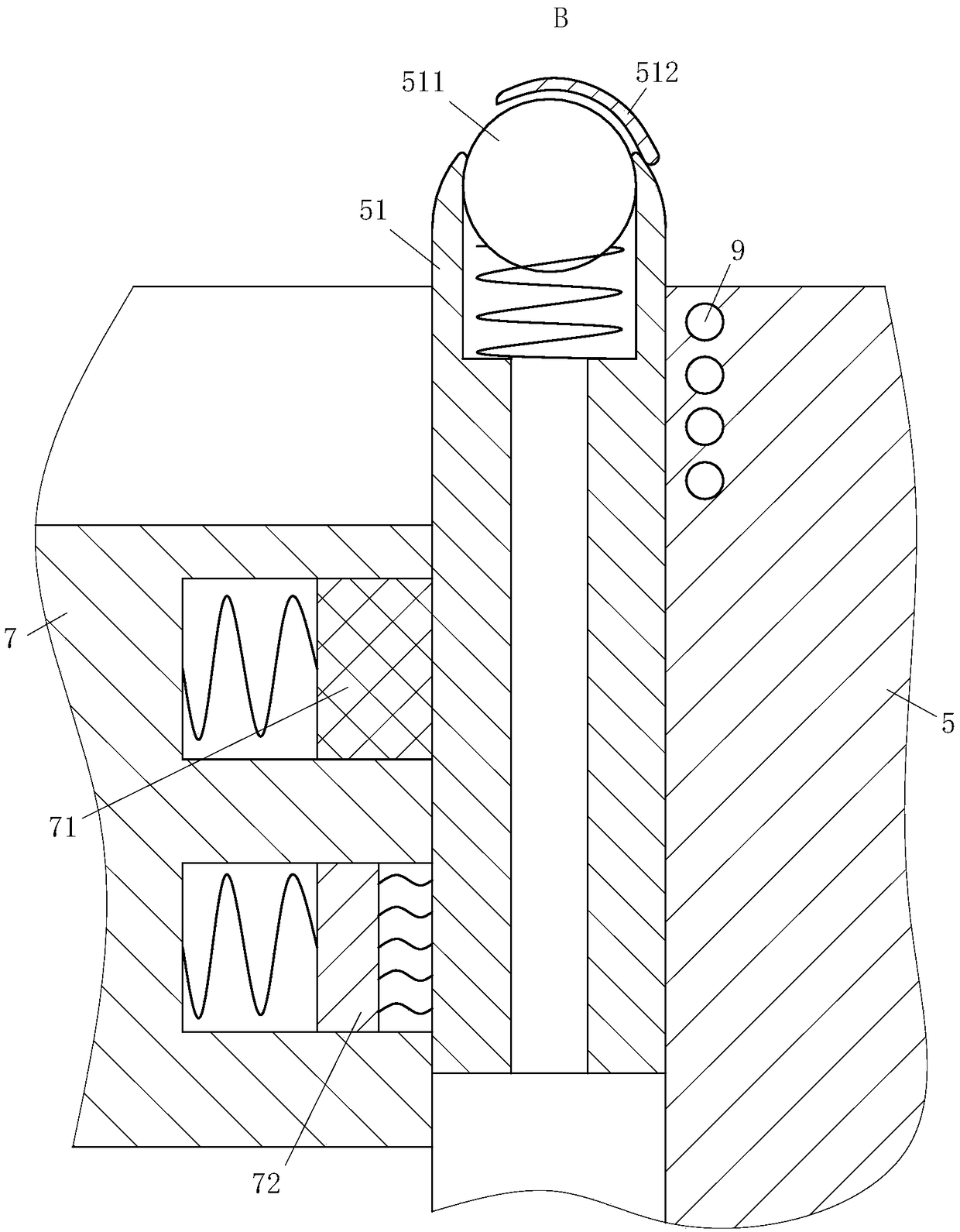
[0022] Such as Figure 1 to Figure 4 As shown, a solar cell wafer manufacturing device according to the present invention includes an upper mounting plate 1, an electric cylinder 2, a No. 1 motor 3, a pressurizing device 4, a mold 5, a mold frame 6, a lifting part 7, and a driver 8. The heater 9, the lower surface of the upper mounting plate 1 is fixedly connected to the base of the electric cylinder 2; the end of the cylinder rod of the electric cylinder 2 is fixedly connected to the non-output end of the No. 1 motor 3; the end of the rotating shaft of the No. 1 motor 3 Fixedly connected to the pressurizing device 4; the pressurizing device 4 includes a pressurizing roller 41 and a No. 1 bracket 42; the shaft end of the No. 1 motor 3 is fixedly c...


PUM


Abstract

The invention relates to the technical field of the solar battery, and specifically is a wafer manufacturing device of the solar battery. The device comprises an upper mounting plate, an electric actuator, a first motor, a pressure device, a mould, a mould rack, a lifting component, a driver and a heater; the end of a cylinder rod of the electric actuator is fixedly connected with a non-output endof the first motor; the end of a rotating shaft of the first motor is fixedly connected with the pressure device; the end of the rotating shaft of the first motor is fixedly connected with the top ofthe middle part of a first bracket; a pressure roller is rotationally installed under the first bracket; and the pressure roller is driven by the electric actuator that is driven by the motor. By adoption of the wafer manufacturing device, the material is not stacked when the wafer is rolled, so as to ensure the uniform density of the rolled wafer; a retractable plate is set on the periphery of the side wall of the mould cavity, so that the melted wafer can be continuously rolled after the wafer is lifted by the lifting component; and thus, the processing efficiency of the wafer is improved.

Description

technical field [0001] The invention belongs to the technical field of solar cell manufacturing, in particular to a solar cell wafer manufacturing device. Background technique [0002] Wafer refers to the silicon chip used in the production of silicon semiconductor integrated circuits. Wafer is the carrier used in the production of integrated circuits. In general, wafers refer to single crystal silicon wafers. Wafer is the most commonly used semiconductor material. According to its diameter, it is divided into 4 inches, 5 inches, 6 inches, 8 inches and other specifications. Recently, 12 inches or even larger specifications have been developed. The larger the wafer, the more ICs that can be produced on the same wafer, which can reduce costs; but the requirements for material technology and production technology are higher, such as uniformity and so on. It is generally believed that the larger the diameter of the silicon wafer, it means that the fab has better technology. In ...

Claims


Application Information

Patent Timeline
IPC IPC(8): H01L21/67H01L31/18B08B1/00
CPCH01L31/1804H01L21/67092B08B1/12Y02E10/547Y02P70/50
Inventor 王青江振
Owner 厦门市信邦威科技有限公司
Why Eureka
Try Eureka