Four-wafer LED display lamp bead structure

A technology of LED display lights and chips, which is applied in the direction of electrical components, electrical solid devices, circuits, etc., can solve the problems of small LED size requirements, ordinary circuit boards cannot meet the needs of circuits at the same time, and the color gamut of three-primary-color LEDs cannot meet the requirements, etc. Achieve the effect of improving display color saturation, displaying brightness and vividness, and enhancing color fidelity

Pending Publication Date: 2018-10-23
山西高科华兴电子科技有限公司
View PDF9 Cites 1 Cited by
  • Summary
  • Abstract
  • Description
  • Claims
  • Application Information

AI Technical Summary

Problems solved by technology

The requirements for the size of the LED are getting smaller and smaller; at the same time, the requirements for the color saturation of the LED are also getting higher and higher, and the color gamut of the traditional three-primary-color LED can no longer meet the requirements.
[0004] At present, as the light intensity of LED lights continues to increase, and the light color requirements are becoming more and more abundant, it is necessary to integrate LED chips with different light-emitting colors (red, green, blue, and white) into a small area. Optical LED chips are widely used in required fields due to their high luminous efficiency. In this way, single and double chips with different electrodes can be integrated in a small area. Ordinary circuit boards cannot meet the requirements of LED heat conduction and the coexistence of single and double electrode chips. need

Method used


Image

  • Four-wafer LED display lamp bead structure
  • Four-wafer LED display lamp bead structure
  • Four-wafer LED display lamp bead structure

Examples


Embodiment 1

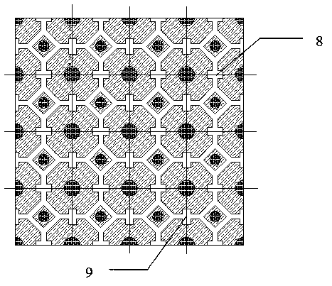
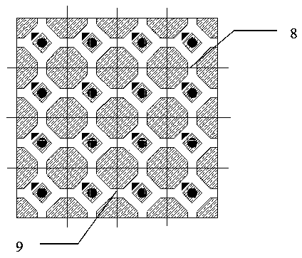
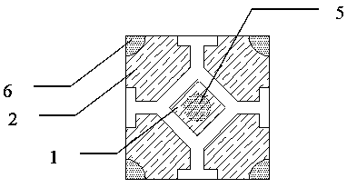
[0028] Image 6 Among them, the LED red chip 13 and the LED yellow chip 14 are bonded on two adjacent non-common level die bonding regions 2 in a vertical structure with conductive silver glue, and the LED blue chip 11 and the LED chip are bonded with insulating glue. The green chip 12 is bonded to the remaining two non-public die bonding areas 2 in a horizontal structure; the whole PCB with the chip fixed and the bonding wire bonded is put into a high-temperature molding mold, and resin is added, and the 150-220 tons of hydraulic pressure mold clamping, under the condition of 100-2220 ℃ mold temperature heating, the resin is initially cured, after the mold is opened, the semi-finished board that has been molded is taken out, baked in an environment of 130-200 ℃, so that the molded The resin is completely cured; transfer to the cutting process, fix it by sticking a film on the back of the semi-finished PCB, and start cutting according to the row cutting line 8 and column cutti...

Embodiment 2

[0030] like Figure 7 As shown, the LED red chip 13 and the LED yellow chip 14 are bonded on the two non-common level die-bonding regions 2 at the diagonal with a vertical structure with conductive silver glue, and the LED blue chip 11 and the LED blue chip 11 are bonded with insulating glue. The LED green chip 12 is bonded on the remaining two non-common level die-bonding bonding regions 2 in a horizontal structure; other steps are the same as in Embodiment 1.

[0031] like Figure 8As shown, the four-crystal lamp bead arranged according to 2R1G1B splits one unit of four-crystal LED into four independent LED units. Each LED unit reproduces the corresponding primary color information of four adjacent pixels in a time-division multiplexing manner, and the LEDs are equally spaced and uniformly distributed among each other. Advantages The virtual pixel density is increased to 4 times; the effective visual pixel density can be increased by up to 4 times.


PUM


Abstract

The invention discloses a four-wafer LED display lamp bead structure comprising four LED wafers, a PCB substrate and a circuit arranged on the substrate. The PCB substrate is composed of a plurality of unit substrates with square structures; common-level bonding regions are arranged at the centers of the unit substrates; non-common-level die bonding regions are arranged at four corners of the unitsubstrates; and common-level bonding pads and non-common-level bonding pads are arranged at the backs of the unit substrates. The common-level bonding regions are connected with the common-level bonding pads by common-level conduction holes; and the non-common-level die bonding regions are connected with the non-common-level bonding pads through surface-copper-plated conduction holes in a one-to-one correspondence manner. LED wafers with four different kinds of colors are pasted to the non-common-level die bonding regions. According to the invention, color combination of four primary colors is realized; the color fidelity of the LED display screen is improved substantially; the connection line is optimized; and the heat conduction requirement of the LED is met.

Description

technical field [0001] The invention relates to an LED package display device, in particular to a four-crystal LED display lamp bead structure. Background technique [0002] As a new type of high-efficiency solid light source, semiconductor lighting has significant advantages such as long life, energy saving, environmental protection, and safety. It will become another leap in the history of human lighting after incandescent lamps and fluorescent lamps. The upgrading of the industry and other industries has huge economic and social benefits. For this reason, semiconductor lighting is generally regarded as one of the most promising emerging industries in the 21st century, and it is also one of the most important commanding heights in the field of optoelectronics in the next few years. Due to its energy-saving, environmental protection, safety and other advantages, light-emitting diodes have been widely used in lighting, electronic devices and other fields, and the applicatio...

Claims


Application Information

Patent Timeline
Patent Type & Authority Applications(China)
IPC IPC(8): H01L25/075H01L33/48H01L33/62
CPCH01L25/0753H01L33/48H01L33/62
Inventor 马洪毅
Owner 山西高科华兴电子科技有限公司
Why Eureka
Try Eureka