Resistive layer self-gating resistive random access memory as well as building method and application thereof

A technology of resistive memory and construction method, applied in the direction of electrical components, etc., to achieve the effect of perfect compatibility

Active Publication Date: 2018-11-02
金雪尚呈(杭州)科技有限公司
View PDF5 Cites 6 Cited by
  • Summary
  • Abstract
  • Description
  • Claims
  • Application Information

AI Technical Summary

Problems solved by technology

Although there are some work reports on 1R in the world at present, there are only a limited number of materials that can realize both the resistive layer (resistance change layer) and the gating function (such as SiO x and TaO x etc.); in the prior art, there is no gating structure or device based on universal physical principles, which breaks through material limitations to a certain extent

Method used


Image

  • Resistive layer self-gating resistive random access memory as well as building method and application thereof
  • Resistive layer self-gating resistive random access memory as well as building method and application thereof
  • Resistive layer self-gating resistive random access memory as well as building method and application thereof

Examples


Embodiment 1

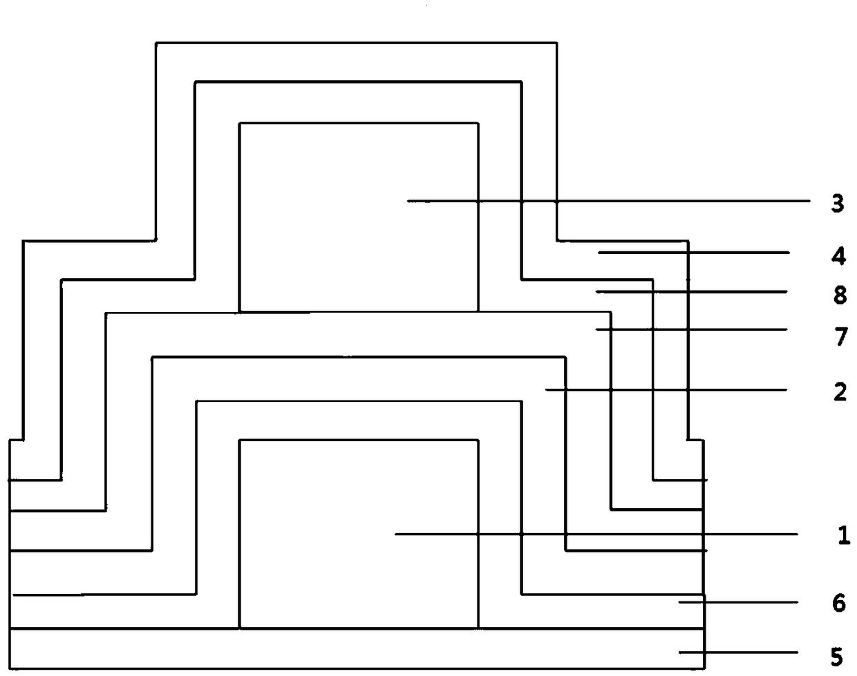
[0063] A resistive variable layer self-selection resistive variable memory, comprising a stacked layer; the stacked layer includes a fourth Hf layer 4, a fourth Si 3 N 4 Layer 8, third Hf layer 3, third Si 3 N 4 Layer 7, second Hf layer 2, second Si 3 N 4 Layer 6, first Hf layer 1 and first Si 3 N 4 Layer 5; the left and right sides of the stacked layer are respectively provided with a bottom electrode and a top electrode; the bottom electrode and the fourth Si 3 N 4 Layer 8, the third Si 3 N 4 Layer 7 communicates with the second Hf layer 2 and is arranged on the upper surface of the second Hf layer 2; the top electrode communicates with the entire stack layer and is arranged on the first Si 3 N 4 top surface of layer 5.

[0064] First Si 3 N 4 The thickness of layer 5 is 25nm; the thickness of the first Hf layer 1 is 110nm; the second Si 3 N 4 The thickness of layer 6 and the second Hf layer 2 is 25nm; the third Si 3 N 4 The thickness of layer 7 is 25nm; the...

Embodiment 2

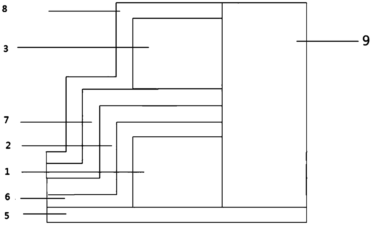
[0067] The resistive variable layer self-selectable resistive variable memory as described in Embodiment 1, the difference is that the resistive variable layer self-selectable resistive variable memory comprises two stacked layers arranged side by side; the top electrode is a bit line; the for the word line.

Embodiment 3

[0069] A method for constructing a resistive variable layer self-selecting resistive variable memory as described in Embodiment 1, comprising the following steps:

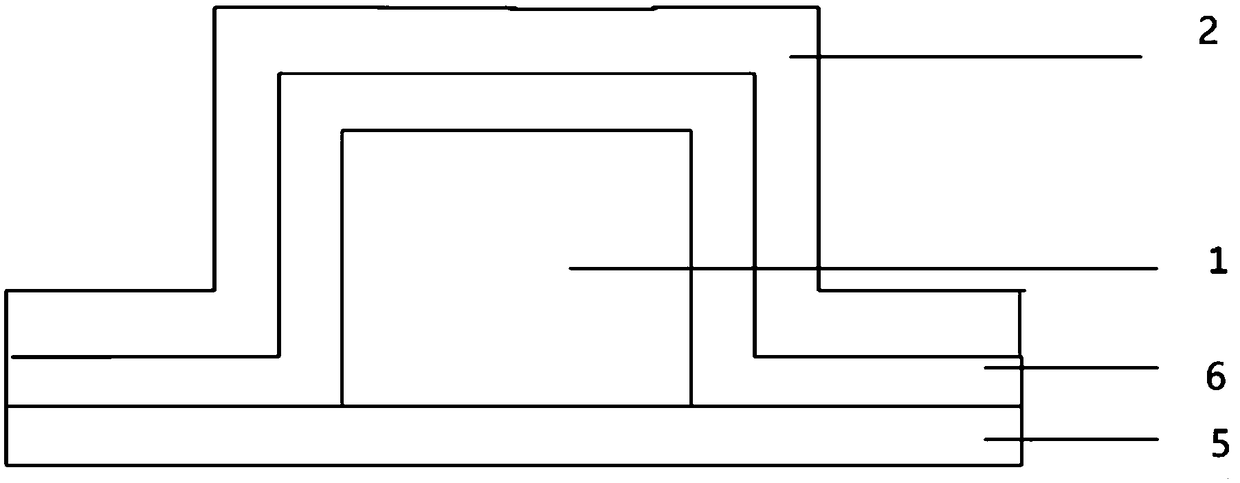
[0070] 1) Deposit the first Si on the substrate 3 N 4 Layer 5; depositing the first Si on the substrate 3 N 4 Layer 5 is realized by CVD method; the substrate is a Si substrate;

[0071] 2) In the first Si 3 N 4 Deposit the first Hf layer 1 on the layer 5, then perform photolithography and lift-off treatment; 3 N 4 The deposition of the first Hf layer 1 on the layer 5 is achieved by a DC sputtering method.

[0072] 3) Deposit the second Si sequentially on the first Hf layer 1 3 N 4 Layer 6, the second Hf layer 2; as figure 1 shown. Second Si 3 N 4 Layer 6 is deposited by CVD method and the second Hf layer 2 is deposited by sputtering.

[0073] 4) Deposit the third Si on the second Hf layer 2 3 N4 Layer 7, according to the method of step 2), 3) in the third Si 3 N 4 Deposit the third Hf layer 3, the...


PUM


Abstract

The invention relates to a resistive layer self-gating resistive random access memory as well as a building method and application thereof. The resistive random access memory comprises an overlappinglayer, wherein the overlapping layer comprises a fourth Hf layer, a fourth Si<3>N<4> layer, a third Hf layer, a third Si<3>N<4> layer, a second Hf layer, a second Si<3>N<4> layer, a first Hf layer anda first Si<3>N<4> layer which are arranged in sequence from outside to inside. During 1R array gating based on a homogeneous HfO<x> base, a resistive layer is taken as a gating layer, so that an extra third gating device is prevented from being introduced. An asymmetrical structure is machined based on micro-nano for filling (or hollowing), a depletion region is formed on the periphery of a filling region under the micro-nano scale, and the depletion region dynamically changes along with an external electric field. A self-gating effect is achieved according to the universal physical principle. Thus, the resistive random access memory is not limited to the HfO<x> material, but also suitable for all materials capable of forming the depletion region.

Description

technical field [0001] The invention relates to a resistive variable layer self-selecting resistive variable memory and its construction method and application, belonging to the technical field of resistive variable memory array gate. Background technique [0002] In recent years, with the rise of big data and artificial intelligence, resistive random access memory (RRAM) has shown great application prospects. For example, its application in neuromorphic chips and large-scale high-integration density data storage. Due to its simple two-terminal structure and the practical advantages of modulating storage through resistance changes, it has natural advantages in miniaturization and high-density integration. In order to fully realize these advantages, it is necessary to make the RRAM in the form of a crossbar array, so as to effectively exert its high-density storage and the function of bionic brain synapses. However, under the cross-array structure, there is a well-known bas...

Claims


Application Information

Patent Timeline
Patent Type & Authority Applications(China)
IPC IPC(8): H01L45/00
CPCH10N70/801H10N70/883H10N70/026H10N70/011
Inventor 蒋然季昊张鑫磊
Owner 金雪尚呈(杭州)科技有限公司
Why Eureka
Try Eureka