

QLED device, display device and preparation method of display device
A device and interface modification technology, which is applied in semiconductor/solid-state device manufacturing, electric solid-state devices, semiconductor devices, etc., can solve the problems of short service life, unbalanced carrier injection, low power efficiency, etc., and achieve less transmission loss, The effect of improving the overall efficiency and reducing the driving voltage
- Summary
- Abstract
- Description
- Claims
- Application Information
AI Technical Summary
Problems solved by technology
Method used
Image

Examples
Embodiment 1
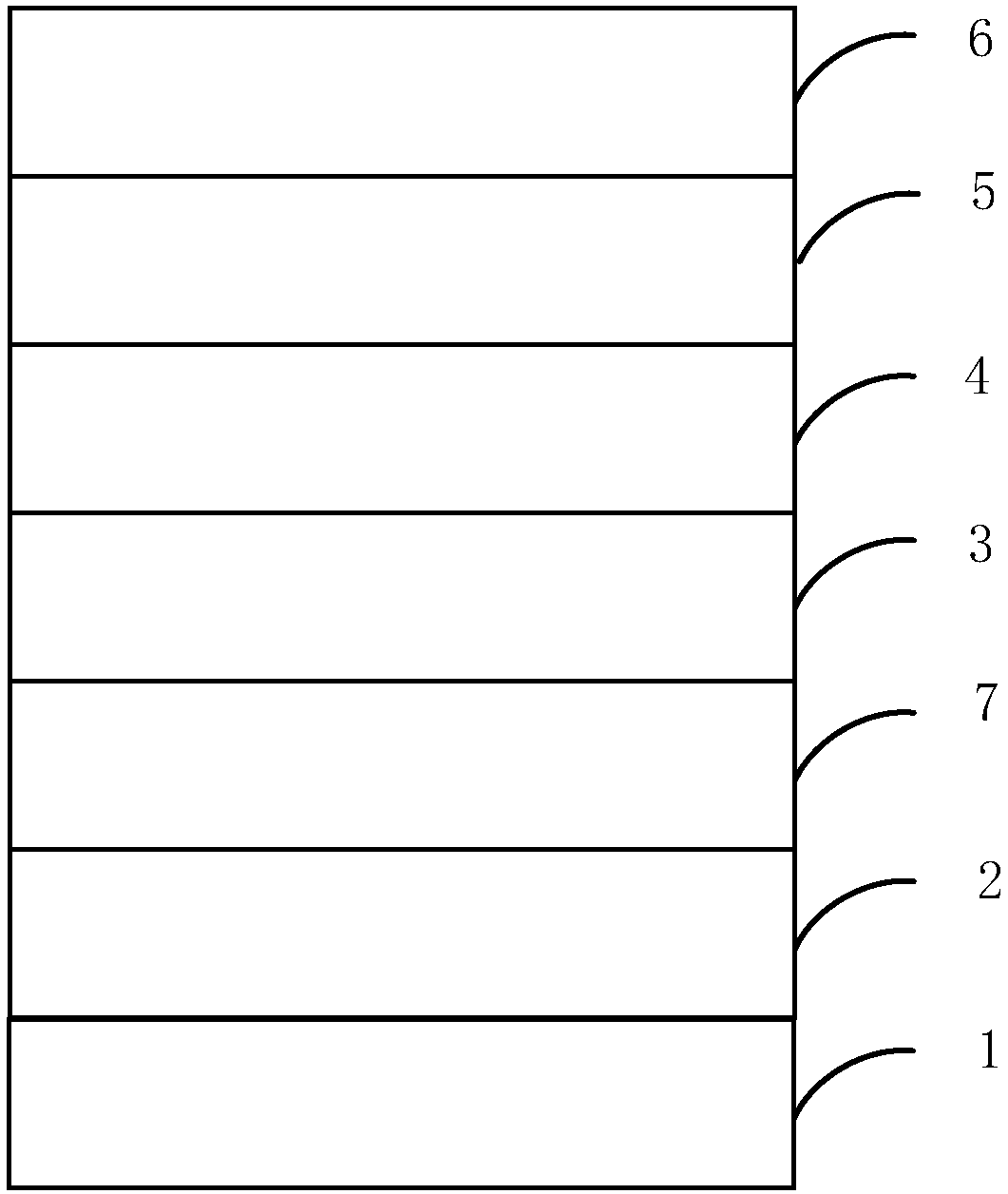
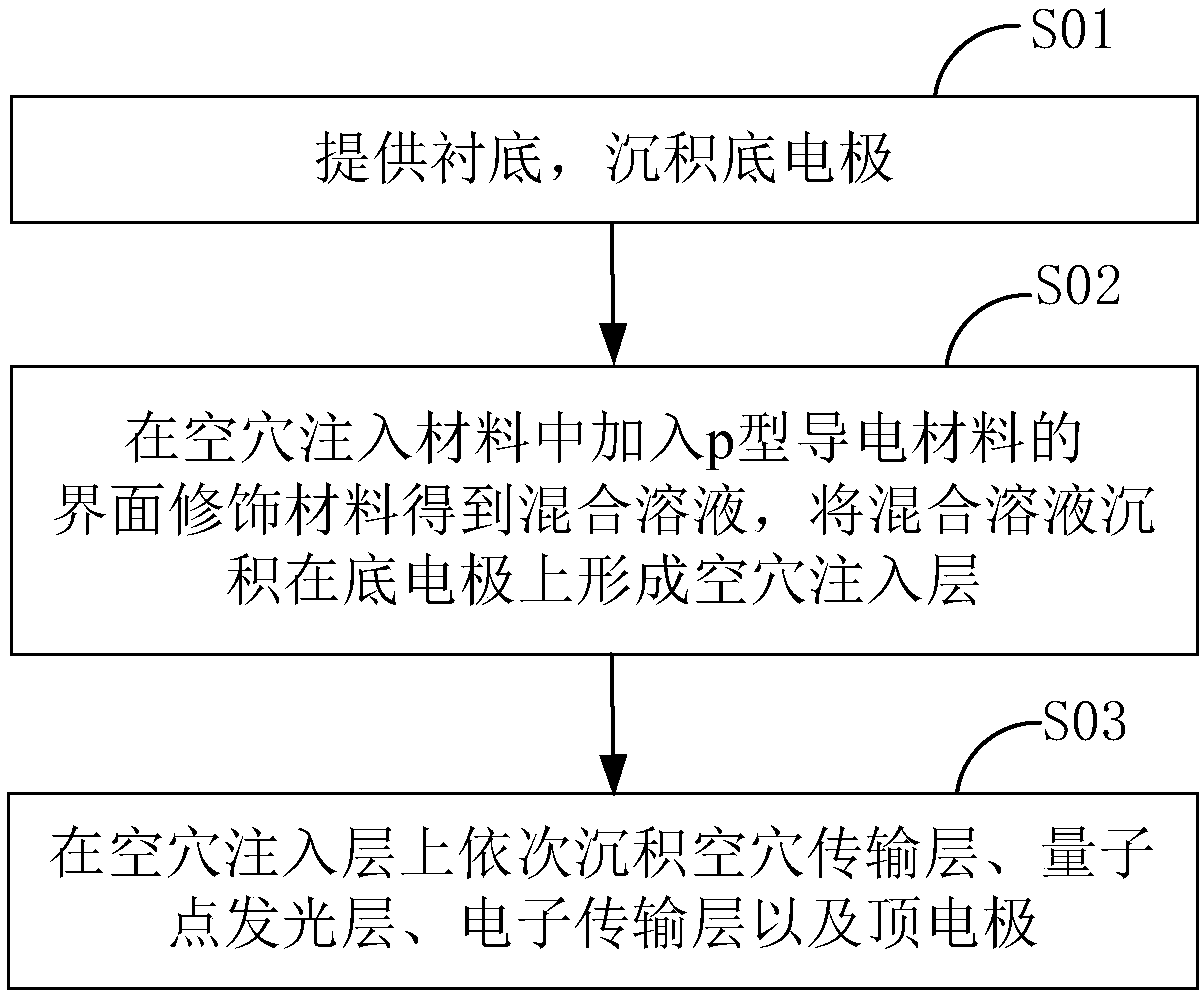
[0034] A QLED device, comprising a substrate 1, a bottom electrode 2, a hole transport layer 3, a quantum dot light-emitting layer 4, an electron transport layer 5 and a top electrode 6 arranged in sequence, and also includes a 5wt% doped by PEDOT:PSS:PFI Hole injection layer 7 made of DMSO. Wherein, the substrate 1 is a glass substrate; the material of the bottom electrode 2 is ITO, and the thickness is 120nm; the thickness of the hole injection layer 7 is 40nm, and the weight ratio of PEDOT:PSS:PFI is 1:2.5:11.2; the hole transport layer The material of 3 is TFB with a thickness of 25nm; the material of quantum dot light-emitting layer 4 is CdSe / ZnS QDs with a thickness of 40nm; the material of electron transport layer 5 is nano-zinc oxide with a thickness of 20nm; the material of top electrode 6 is Al.
[0035] In the embodiment of the present invention, PEDOT:PSS:PFI is doped with 5wt% DMSO, so that the work function of the hole injection layer 7 is improved from 4.7eV com...
Embodiment 2
[0037]A QLED device, comprising a substrate 1, a bottom electrode 2, a hole transport layer 3, a quantum dot luminescent layer 4, an electron transport layer 5 and a top electrode 6 arranged in sequence, also includes a PEDOT:PSS film doped with a thickness of 40nm A hole injection layer 7 made of 0.1 wt% multi-walled carbon nanotubes. Among them, the substrate 1 is a glass substrate; the material of the bottom electrode 2 is ITO with a thickness of 120nm; the material of the hole transport layer 3 is TFB with a thickness of 25nm; the material of the quantum dot light-emitting layer 4 is CdSe / ZnS QDs with a thickness of 40nm; the material of the electron transport layer 5 is nano zinc oxide with a thickness of 20nm; the material of the top electrode 6 is Al.
[0038] In this embodiment, by doping 0.1wt% multi-walled carbon nanotubes through the PEDOT:PSS thin film, the electrical conductivity of the hole injection layer 7 is improved compared to the electrical conductivity of ...
Embodiment 3
[0040] A QLED device, comprising a substrate 1, a bottom electrode 2, a hole transport layer 3, a quantum dot luminescent layer 4, an electron transport layer 5 and a top electrode 6 arranged in sequence, also includes a PEDOT:PSS film doped with a thickness of 40nm A hole injection layer 7 made of 6 wt% liquid bromine. Among them, the substrate 1 is a glass substrate; the material of the bottom electrode 2 is ITO with a thickness of 120nm; the material of the hole transport layer 3 is TFB with a thickness of 25nm; the material of the quantum dot light-emitting layer 4 is CdSe / ZnS QDs with a thickness of 40nm; the material of the electron transport layer 5 is nano zinc oxide with a thickness of 20nm; the material of the top electrode 6 is Al.
[0041] In this embodiment, the PEDOT:PSS thin film is doped with 6wt% liquid bromine, so that the electrical conductivity of the hole injection layer 7 is increased by 300 times compared to the electrical conductivity of the hole inject...
PUM
| Property | Measurement | Unit |
|---|---|---|
| Thickness | aaaaa | aaaaa |
| Thickness | aaaaa | aaaaa |
| Thickness | aaaaa | aaaaa |
Abstract
Description
Claims
Application Information