A preparation method of a silicon-based microneedle array patch

A microneedle array, silicon-based technology, applied in the field of microneedles, can solve the problems of complex process, poor puncturing ability, and difficult processing, and achieve the effects of simple process, simple processing and good compatibility

Active Publication Date: 2018-11-06
上海揽微医学科技有限公司
View PDF14 Cites 4 Cited by
  • Summary
  • Abstract
  • Description
  • Claims
  • Application Information

AI Technical Summary

Problems solved by technology

[0008] The invention aims to overcome the problems in the prior art that the process is complicated, the processing is difficult, and the pinhole is located at the center of the needle body, and the puncture ability is poor. Needle tip, strong puncture ability, a silicon-based microneedle array patch preparation method that uses micro-nano processing technology to realize large-area patch type

Method used


Image

  • A preparation method of a silicon-based microneedle array patch

Examples


Embodiment 1

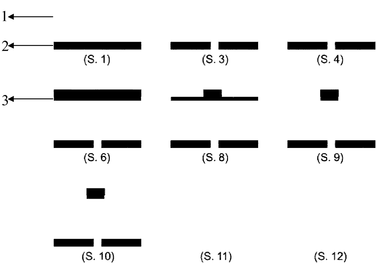
[0041] A method for preparing a silicon-based microneedle array patch, the preparation method comprising preparation of micropores and preparation of needle tips, wherein:

[0042] Micropores are prepared by the following steps:

[0043] S.1 Coating AZP 4620 positive photoresist on the back of the silicon wafer;

[0044] S.2 Put the silicon wafer coated with AZP 4620 positive photoresist on the backside and bake it on a hot plate at 90°C for 5 minutes, and the thickness of the photoresist obtained is 5 microns;

[0045] S.3 The photolithography light intensity is 2.7mW / cm 2 , photolithographic exposure was carried out under the condition of lithography time 250s, and then developed with AZ300 MIF developer for 100s, after the development was completed, rinsed with deionized water for 1 minute to prepare a hole array with a hole diameter of 30 microns;

[0046] S.4 Deep silicon etching, forming deep holes in the silicon wafer;

[0047] The needle tip is prepared by the followi...

Embodiment 2

[0057] A method for preparing a silicon-based microneedle array patch, the preparation method comprising preparation of micropores and preparation of needle tips, wherein:

[0058] Micropores are prepared by the following steps:

[0059] S.1 Coating AZP 4620 positive photoresist on the back of the silicon wafer;

[0060] S.2 Put the silicon wafer coated with AZP 4620 positive photoresist on the backside and bake it on a hot plate at 110°C for 1 minute, and the thickness of the obtained photoresist is 15 microns;

[0061] S.3 The photolithography light intensity is 3.0mW / cm 2 , photolithographic exposure was carried out under the condition of lithography time 150s, and then developed with AZ300 MIF developer for 100s, after development, rinsed with deionized water for 3 minutes to prepare a hole array with a hole diameter of 30 microns;

[0062] S.4 Deep silicon etching, forming deep holes in the silicon wafer;

[0063] The needle tip is prepared by the following steps:

[...

Embodiment 3

[0073] A method for preparing a silicon-based microneedle array patch, the preparation method comprising preparation of micropores and preparation of needle tips, wherein:

[0074] Micropores are prepared by the following steps:

[0075] S.1 Coating AZP 4620 positive photoresist on the back of the silicon wafer;

[0076] S.2 Put the silicon wafer coated with AZP 4620 positive photoresist on the backside and bake it on a hot plate at 100°C for 2 minutes, and the thickness of the obtained photoresist is 8 microns;

[0077] S.3 The photolithography light intensity is 2.8mW / cm 2 , photolithographic exposure was carried out under the condition of lithography time 200s, and then developed with AZ300 MIF developer for 200s, after the development was completed, rinsed with deionized water for 2 minutes to prepare a hole array with a hole diameter of 30 microns;

[0078] S.4 Deep silicon etching, forming deep holes in the silicon wafer;

[0079] The needle tip is prepared by the fol...


PUM

PropertyMeasurementUnit
thicknessaaaaaaaaaa
diameteraaaaaaaaaa
thicknessaaaaaaaaaa

Abstract

A preparation method of a silicon-based microneedle array patch is disclosed. The method includes S.1) coating the back of a silicon wafer with a photoresist; S.2) baking the silicon wafer; S.3) photoetching, exposing, and developing to prepare a hole array; S.4) performing deep silicon etching to form deep holes in the silicon wafer; S.5) covering the front surface of the silicon wafer with an aluminum film layer through electron beam evaporation; S.6) coating the front surface of the silicon wafer with the photoresist; S.7) baking the silicon wafer; S.8) photoetching, exposing, and developing to prepare a photoresist cylinder array; S.9) immersing the silicon wafer into an aluminum corrosive liquid to remove the excess aluminum film, and rinsing; S.10) performing deep silicon etching toobtain a silicon needle tip blank array, with aluminum being adopted as an etching template; S.11) removing the photoresist and the aluminum film; and S.12) immersing the silicon wafer into a corrosive liquid to obtain a silicon-based microneedle array. Beneficial effects of the method are that (1) a preparation process is greatly simplified and processing is simple; (2) micropores deviate from the centers of needle tips and piecing capability is enhanced; and (3) subsequent secondary processing can be performed conveniently.

Description

technical field [0001] The invention relates to a microneedle, in particular to a method for preparing a silicon-based microneedle array patch. Background technique [0002] (1) Injection is an important method and way of modern medical diagnosis. Through injection, people can perform various medical procedures such as administering drugs, adding loads, extracting tissues, and monitoring body fluids. Traditional injection is a tense and painful process, which often causes discomfort to patients. At the same time, needles can also cause damage to organs and skin, cross-infection and other problems. In the past ten years, people have proposed the concept of microneedles in order to solve the dilemma of syringes. The percutaneous micro-injection / sampling method of the microneedle effectively reduces the metabolic burden of the liver / digestive tract, liver injury toxicity, cross-infection and other problems. Moreover, the injection and extraction of microneedles are simple an...

Claims


Application Information

Patent Timeline
Patent Type & Authority Applications(China)
IPC IPC(8): B81C1/00
CPCB81C1/00087B81C1/00111B81C1/00396B81C1/00539
Inventor 张鉴张雪峰姚小莉邓萌萌
Owner 上海揽微医学科技有限公司
Why Eureka
Try Eureka