Multi-transmission peak plasma filter based on MIM waveguide coupling cavity structure

A plasma and coupled cavity technology, applied in the field of micro-nano optoelectronics, can solve the problems of small number of transmission peaks, low transmittance, limited application range, etc., and achieve the effect of improving utilization, good performance, and easy integration

Active Publication Date: 2018-11-06
GUILIN UNIV OF ELECTRONIC TECH
View PDF5 Cites 5 Cited by
  • Summary
  • Abstract
  • Description
  • Claims
  • Application Information

AI Technical Summary

Problems solved by technology

[0005] The present invention mainly aims at the problem that the traditional filter and the surface plasmon optical filter have few transmission peaks and low transmittance, which leads to the limited application range, and proposes a multi-transmission peak plasma filter based on the MIM waveguide coupling cavity structure device

Method used


Image

  • Multi-transmission peak plasma filter based on MIM waveguide coupling cavity structure
  • Multi-transmission peak plasma filter based on MIM waveguide coupling cavity structure
  • Multi-transmission peak plasma filter based on MIM waveguide coupling cavity structure

Examples


Embodiment Construction

[0029] In order to make the purpose, technical solution and advantages of the present invention clearer, the present invention will be further described in detail below in combination with specific examples and with reference to the accompanying drawings.

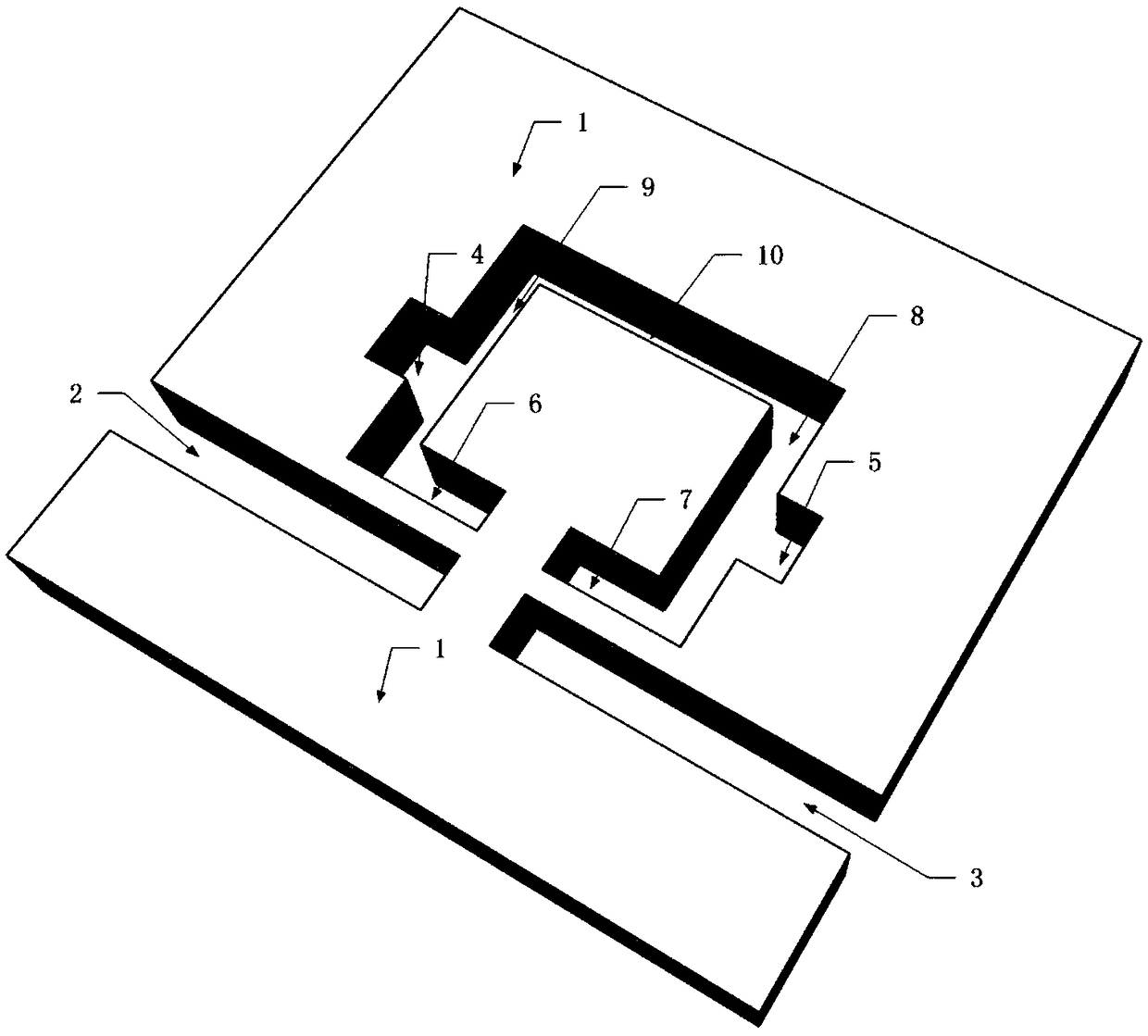
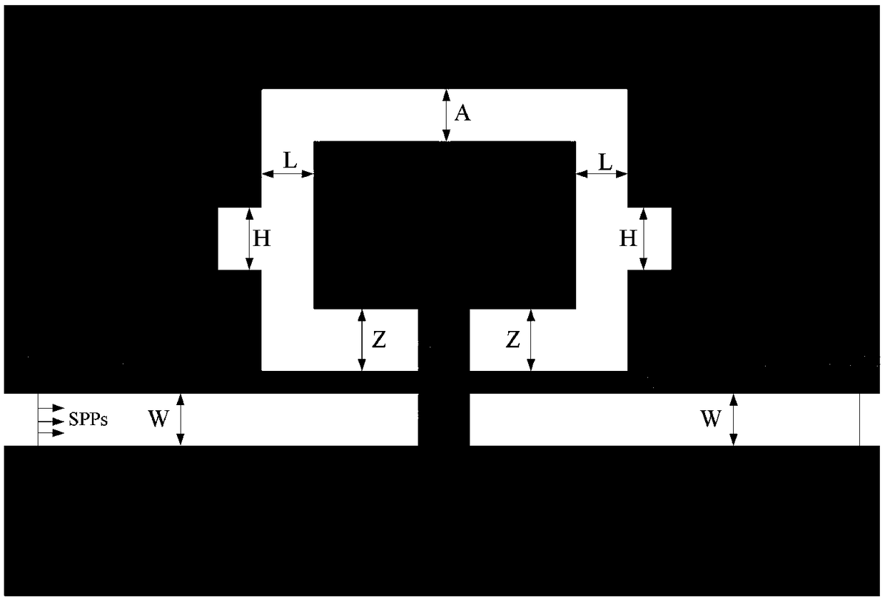
[0030] figure 1 It is a three-dimensional structural schematic diagram of a multi-transmission peak plasma filter based on the MIM waveguide coupling cavity structure of the present invention. The overall structure is mainly composed of a metal film 1 and a plurality of slit-hole structural units, and these multiple slit-hole structural units are evenly penetrated on the metal film. In order to obtain the best filtering performance, the length of the metal film is 2000nm, the width is 2000nm, and the thickness is 100nm. The plurality of slit structural units are mainly composed of waveguides and resonant cavities. The waveguide is divided into an incident waveguide 2 and an outgoing waveguide 3; the resonant cavity is com...


PUM

PropertyMeasurementUnit
Lengthaaaaaaaaaa
Widthaaaaaaaaaa
Lengthaaaaaaaaaa

Abstract

The invention discloses a multi-transmission peak plasma filter based on a MIM waveguide coupling cavity structure, which is characterized in that the multi-transmission peak plasma filter mainly comprises a metal film and a plurality of slit structural units formed on the metal film; the slit structural units are composed of a plurality of lateral rectangular slits and a plurality of longitudinalrectangular slits which pass through upper and lower surfaces of the metal film; two lateral rectangular slit structural units at the same level of the lower end of the metal film are an incident tube and an exit tube of a waveguide; and three lateral rectangular slits and four longitudinal rectangular slit structural units above the waveguide in the metal film form a unified overall resonant cavity. The filter structure of the invention has tunable and high transmittance characteristics in the infrared band; the size of a transmission spectrum and a frequency selection position can be effectively adjusted by changing relevant parameters of the structure, so that the output characteristics of the filter are changed. The research results show that the highest transmittance can reach 93%, the transmittance of each transmission peak is 75% or more, the half-height width can reach below 10nm, and the quality factor can reach 122.81. The optimal filtering effect can be obtained by changingthe relevant parameters of the structure. The multi-transmission peak filter device has the advantages of wide application range, high utilization rate, easy integration, flexible application, etc.,and thus has good application prospect in all-optical networks.

Description

(1) Technical field [0001] The invention belongs to the technical field of micro-nano optoelectronics, and in particular relates to a multi-transmission peak plasma filter based on an MIM waveguide coupling cavity structure. (2) Background technology [0002] Surface plasmon polaritons (Surface Plasmon Polartions, SPPs) are electromagnetic surface waves formed by the interaction of free electrons and photons incident on the metal surface, which propagate along the metal-dielectric surface and perpendicular to the metal interface to both The side decays exponentially. Surface plasmons have good local characteristics, which can confine the electromagnetic field energy in the sub-wavelength range, and can overcome the diffraction limit of optics, enabling the realization of optical integrated devices in the micro-nano range. [0003] In recent years, with the gradual maturity of nanotechnology, the communication technology using light as the carrier of information transmission...

Claims


Application Information

Patent Timeline
IPC IPC(8): G02B6/293G02B26/00
CPCG02B6/29323G02B26/007
Inventor 杨宏艳杨秀华韦柳夏苑立波
Owner GUILIN UNIV OF ELECTRONIC TECH
Why Eureka
Try Eureka