Supercharge Your Innovation With Domain-Expert AI Agents!

Solid-state light source lighting system integrated packaging structure and manufacturing method

A light-emitting system, solid-state light source technology, applied in the direction of electric solid-state devices, semiconductor devices, electrical components, etc., can solve problems such as unfavorable lighting effects, large circuit board area, etc., to reduce the area, improve product consistency and stability, reduce high effect

Active Publication Date: 2020-01-07
张琴
View PDF6 Cites 0 Cited by
  • Summary
  • Abstract
  • Description
  • Claims
  • Application Information

AI Technical Summary

Problems solved by technology

[0007] In the current system design, the above three parts are supplied independently. In the design and processing stages, space needs to be reserved on the circuit board for welding and installation, which is not conducive to confirming the lighting effect in advance, and the area occupied by the circuit board is too large.

Method used


Image

  • Solid-state light source lighting system integrated packaging structure and manufacturing method
  • Solid-state light source lighting system integrated packaging structure and manufacturing method
  • Solid-state light source lighting system integrated packaging structure and manufacturing method

Examples


Embodiment

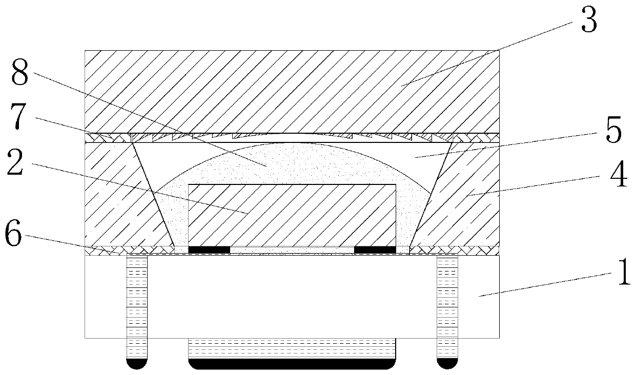
[0065] Such as Figure 1 to Figure 5 As shown, this embodiment provides an integrated packaging structure for a solid-state light source lighting system, the packaging structure includes a light source driver chip 1, a solid-state light-emitting light source chip 2 and a lens 3, and the light source driver chip 1 and the lens 3 are connected through a filler 4 The filler 4 forms a cavity 5 between the light source driving chip 1 and the lens 3 , the solid state light emitting source chip 2 is mounted on the back of the light source driving chip 1 , and the solid state light emitting light source chip 2 is located in the cavity 5 .

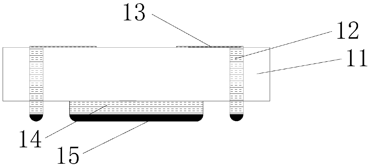
[0066] The light source driving chip 1 is used to control the current and voltage of the solid-state light-emitting light source chip 2, and adjust the luminous intensity of the solid-state light-emitting light source chip 2. It includes a driving chip body 11, and a through hole 12 is provided on the driving chip body 11. Specifically, The through...


PUM


Abstract

The invention discloses a solid-state light source light-emitting system integrated packaging structure and a manufacturing method. The packaging structure comprises a light source driving chip, a solid-state light-emitting light source chip and a lens, wherein the light source driving chip is connected with the lens through a filling piece; a reflecting surface is arranged on the inner side of the filling piece, and the filling piece forms a cavity between the light source driving chip and the lens; and the solid-state light-emitting light source chip is attached to the back surface of the light source driving chip, and the solid-state light-emitting light source chip is located in the cavity. A wafer-level stacking structure is adopted, and the solid-state light-emitting light source chip is attached to the back surface of the light source driving chip, so that the current transmission path is shortened, the power loss is reduced, the assembling precision is improved and micron precision can be achieved, and consistency and stability of products of the solid-state light source light-emitting system are improved; and meanwhile, the throughput of the packaging process is greatly improved, and the packaging manufacturing cost can be greatly lowered.

Description

technical field [0001] The invention relates to an integrated packaging structure of a lighting system, in particular to an integrated packaging structure and a manufacturing method of a solid-state light source lighting system, belonging to the field of packaging of lighting systems. Background technique [0002] In the current solid-state lighting technology, the light source is mainly light-emitting diodes, referred to as LEDs, which are widely used as light sources for lighting and display screens. [0003] The main functional structure of the system includes the following three aspects: [0004] 1) Solid-state light sources, usually light-emitting diodes, LED (Light Emitting Diode), and now laser diodes, LD (Laser Diode), are also commonly used as light sources in detection equipment. [0005] 2) The power drive chip supplies power to the solid-state power supply and performs switching functions; [0006] 3) The light effect adjustment lens, usually a plastic lens, ad...

Claims


Application Information

Patent Timeline
Patent Type & Authority Patents(China)
IPC IPC(8): H01L25/075
CPCH01L25/075
Inventor 张琴
Owner 张琴
Features
  • R&D
  • Intellectual Property
  • Life Sciences
  • Materials
  • Tech Scout
  • Unparalleled Data Quality
  • Higher Quality Content
  • 60% Fewer Hallucinations
Learn More