A kind of preparation method of field emission array cathode

A field emission cathode and emission array technology, which is applied in cold cathode manufacturing, electrode system manufacturing, discharge tube/lamp manufacturing, etc., can solve problems such as poor repeatability, complicated process, and high pollution

Active Publication Date: 2020-10-23
UNIV OF ELECTRONICS SCI & TECH OF CHINA
View PDF6 Cites 0 Cited by
  • Summary
  • Abstract
  • Description
  • Claims
  • Application Information

AI Technical Summary

Problems solved by technology

[0008] Aiming at the defects of complicated process, poor repeatability, high pollution, high cost and other defects in the preparation method of field emission array cathode in the prior art, the present invention provides a method of cutting the cathode substrate to form an initial array by using mechanical processing technology, and then using etching technology Optimizing the shape of the initial array to prepare a pointed array

Method used


Image

  • A kind of preparation method of field emission array cathode
  • A kind of preparation method of field emission array cathode
  • A kind of preparation method of field emission array cathode

Examples


Embodiment 1

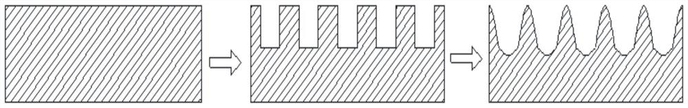
[0030] A method for preparing a field emission array cathode. In this embodiment, polycrystalline lanthanum hexaboride is selected as the cathode material, and the field emission array cathode is prepared by combining wire electric discharge cutting and electrochemical corrosion method. The process flow is as follows figure 2 Shown:

[0031] (1). Polishing and cleaning

[0032] After polishing the polycrystalline lanthanum hexaboride substrate, ultrasonically clean it with deionized water for 15 minutes;

[0033] (2). Wire cutting

[0034] cutting a prismatic primary emitter array on a polycrystalline lanthanum hexaboride substrate by using an electric discharge cutting method;

[0035] The structural parameters of the initial emitter array are mainly as follows: the diameter of the polycrystalline lanthanum hexaboride substrate is 8mm, the thickness of the polycrystalline lanthanum hexaboride substrate is 2.5mm, the length of the emitter edge is 0.25mm, and the emitter slo...

Embodiment 2

[0043] A method for preparing a field emission array cathode. In this embodiment, polycrystalline lanthanum hexaboride is selected as the cathode material, and the field emission array cathode is prepared by combining diamond wire cutting and wet etching:

[0044] (1). Polishing and cleaning

[0045] After polishing the polycrystalline lanthanum hexaboride substrate, ultrasonically clean it with deionized water for 15 minutes;

[0046] (2). Wire cutting

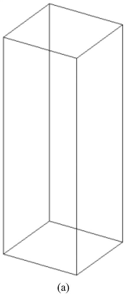
[0047] Use a diamond wire cutting machine to cut out a columnar array on a polycrystalline lanthanum hexaboride substrate. When cutting, use paraffin to fix the lanthanum hexaboride substrate on the cutting board, and then adjust the parameters for cutting;

[0048] The structural parameters of the initial emitter array are mainly as follows: the diameter of the polycrystalline lanthanum hexaboride substrate is 8mm, the thickness of the polycrystalline lanthanum hexaboride substrate is 2.5mm, the length of the emitter edge i...

Embodiment 3

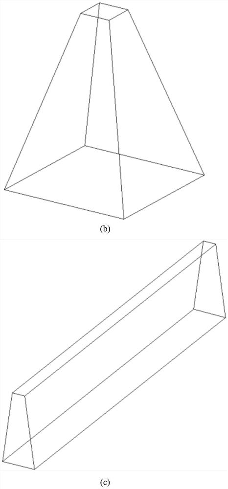
[0054] In this embodiment, a diamond wire cutting machine is used to cut a blade-shaped array on the surface of a polycrystalline lanthanum hexaboride substrate, and the shape of each field emitter in the cut blade-shaped array is like a blade, gradually narrowing from bottom to top (i.e. wide at the bottom and narrow at the top), the blade array obtained by mechanical cutting is as follows Figure 5 As shown in (a), after RIE etching, the top of the field emitter will be sharper, such as Figure 5 (b).


PUM

PropertyMeasurementUnit
diameteraaaaaaaaaa
thicknessaaaaaaaaaa
lengthaaaaaaaaaa

Abstract

The invention discloses a method for preparing a field emission array cathode, which belongs to the technical field of cathode field emission. In the present invention, the field emission cathode substrate is installed on a cutting machine, and the cutting parameters are set to obtain an initial emitter array formed by a prismatic emitter, and the obtained emitter is further etched to form a pointed emitter, thereby obtaining Field emission cathode cone array. The present invention combines mechanical processing technology and etching technology to prepare field emission array cathodes, which simplifies the process flow and reduces production costs compared with the existing photolithography technology combined with etching technology; at the same time, by adjusting mechanical processing parameters and etching process parameters , field emission array cathodes with different array sizes, array heights and array spacings can be obtained, the preparation process is highly controllable, and the use of toxic and harmful reagents is avoided at the same time, which conforms to the concept of modern green and environmental protection; the preparation method of the present invention has good repeatability and is effective It is beneficial to the popularization and application of the field emission array cathode.

Description

technical field [0001] The invention belongs to the technical field of cathode field emission, in particular to a method for preparing a cathode of a field emission array. Background technique [0002] In 1897, R.W. Wood first discovered the field electron emission (FEE) phenomenon. In 1923, W. Schottky conducted in-depth theoretical research on the FEE phenomenon, and put forward the following hypothesis: the external electric field weakens the surface potential barrier, and the barrier height is reduced, so that electrons can escape through the barrier. According to the theory of field electron emission, the main factors affecting the performance of field emission are: local electric field strength and material work function. In the case of a constant macroscopic electric field, the electric field intensity on the surface of the emitter depends on the shape of the emitter and the field enhancement effect caused by the micro-protrusion on the surface; the work function of ...

Claims


Application Information

Patent Timeline
Patent Type & Authority Patents(China)
IPC IPC(8): H01J9/02H01J1/304
CPCH01J1/3042H01J9/025
Inventor 王小菊韩欣延李茂想祁康成曹贵川季子颉
Owner UNIV OF ELECTRONICS SCI & TECH OF CHINA
Why Eureka
Try Eureka