semiconductor integrated circuit with hkmg

An integrated circuit and semiconductor technology, applied in the field of semiconductor integrated circuits, to achieve the effects of improving electrical performance, preventing offset and disturbance, and low cost

Active Publication Date: 2020-11-24
SHANGHAI HUALI INTEGRATED CIRCUTE MFG CO LTD
View PDF3 Cites 0 Cited by
  • Summary
  • Abstract
  • Description
  • Claims
  • Application Information

AI Technical Summary

Problems solved by technology

However, the separation of the work function layers of the PMOS transistor and the NMOS transistor cannot avoid the above-mentioned metal gate boundary effect.

Method used


Image

  • semiconductor integrated circuit with hkmg
  • semiconductor integrated circuit with hkmg
  • semiconductor integrated circuit with hkmg

Examples


Embodiment Construction

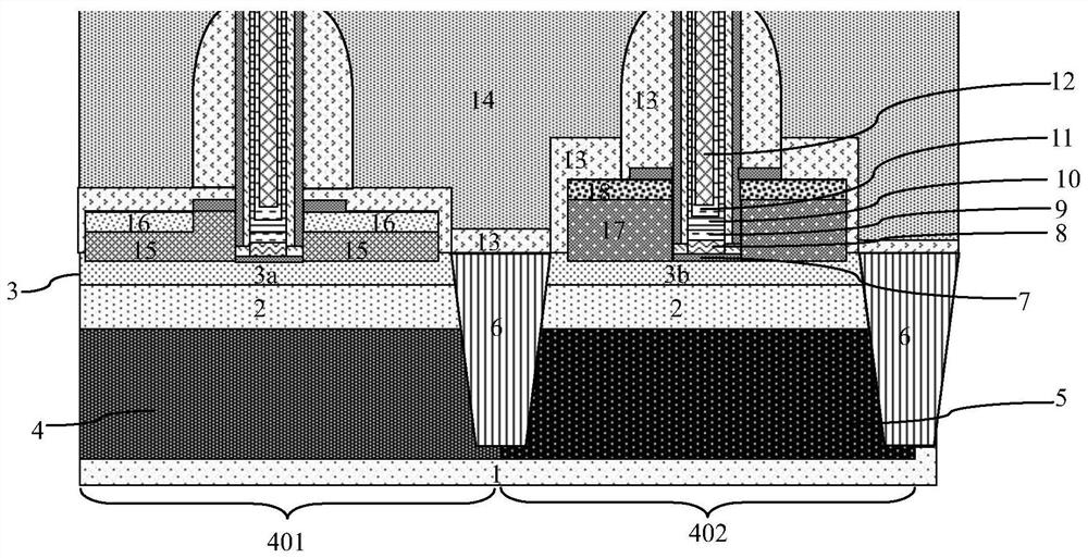
[0051] Such as image 3 Shown is the structural diagram of the semiconductor integrated circuit with HKMG in the embodiment of the present invention; the semiconductor integrated circuit with HKMG in the embodiment of the present invention includes:

[0052] FDSOI substrate structure, the FDSOI substrate comprises a bottom semiconductor layer 1, a buried oxide layer 2 and a top semiconductor layer 3, the buried oxide layer 2 is formed on the surface of the bottom semiconductor layer 1, and the top semiconductor layer 3 is formed on The surface of the buried oxide layer 2 . In the embodiment of the present invention, the bottom semiconductor layer 1 is a bottom silicon layer, the material of the buried oxide layer 2 is silicon oxide, and the top semiconductor layer 3 is a top silicon layer.

[0053] For the FDSOI process, it has the following typical characteristics: the wafer used, that is, the bottom semiconductor layer 1, has a layer of buried oxide (buried oxide, BOX), whi...


PUM

PropertyMeasurementUnit
thicknessaaaaaaaaaa
thicknessaaaaaaaaaa

Abstract

The invention discloses a semiconductor integrated circuit with HKMG, comprising: a semiconductor device is formed on an FDSOI substrate structure, the work function of the work function layer of HKMG tends to the middle value of the forbidden band width of the top semiconductor layer; the FDSOI substrate The bottom structure has an adjustment structure of the threshold voltage of the semiconductor device. The adjustment structure of the threshold voltage of the semiconductor device includes an inversion channel doping structure and a substrate bias application structure. The threshold voltage of the semiconductor device is adjusted by the threshold voltage adjustment structure of the semiconductor device, the influence of the work function layer on the threshold voltage of the semiconductor device is offset, and a semiconductor device with a threshold voltage meeting requirements is formed. The invention can unify the structure of the HKMG of the PMOS transistor and the NMOS transistor, and can eliminate the metal grid boundary effect produced when the HKMG of the PMOS transistor and the NMOS transistor are different.

Description

technical field [0001] The invention relates to a semiconductor integrated circuit, in particular to a semiconductor integrated circuit with HKMG. Background technique [0002] HKMG has a gate dielectric layer with a high dielectric constant (HK) and a metal gate (MG), so it is usually abbreviated as HKMG in the art. Such as figure 1 As shown, it is the layout of the half-bit cell structure of the existing SRAM with HKMG; as figure 2 shown, is the existing along figure 1 The cross-sectional structure diagram of two adjacent first PMOS transistors 302 and second NMOS transistors 301 on the AA line in the figure, the existing cell structure of the SRAM with HKMG SRAM includes two adjacent shared metal gates 109 of the first A PMOS transistor 302 and a second NMOS transistor 301, the HKMG of the first PMOS transistor 302 includes a gate dielectric layer and a metal gate 109, and there is a first work function layer 106 and a second metal gate between the gate dielectric lay...

Claims


Application Information

Patent Timeline
Patent Type & Authority Patents(China)
IPC IPC(8): H01L27/092H01L27/11H01L21/8238
CPCH01L27/092H01L21/823828H10B10/125
Inventor 徐翠芹刘巍
Owner SHANGHAI HUALI INTEGRATED CIRCUTE MFG CO LTD
Why Eureka
Try Eureka