Perovskite composite film, light emitting diode and preparation method of perovskite composite film

A technology of light-emitting diodes and composite thin films, applied in semiconductor/solid-state device manufacturing, electrical components, circuits, etc., can solve problems such as low quantum efficiency and achieve the effect of improving film formation

Inactive Publication Date: 2018-11-13
SOUTHWEST UNIVERSITY
View PDF4 Cites 3 Cited by
  • Summary
  • Abstract
  • Description
  • Claims
  • Application Information

AI Technical Summary

Problems solved by technology

[0005] In order to solve the problem of low quantum efficiency in light-emitting devices, bis(2-(4,6-difluorophenyl)-pyridinato-N,C2') picolinate (FIrpic), a phosphorescent material with nearly 100% internal quantum efficiency, was used as In TmPyPB and CsPbBr 3 Sensitizers for energy transfer between perovskites

Method used


Image

  • Perovskite composite film, light emitting diode and preparation method of perovskite composite film
  • Perovskite composite film, light emitting diode and preparation method of perovskite composite film
  • Perovskite composite film, light emitting diode and preparation method of perovskite composite film

Examples


Embodiment Construction

[0014] Embodiments of the technical solutions of the present invention will be described in detail below in conjunction with the accompanying drawings. The following examples are only used to illustrate the technical solutions of the present invention more clearly, and therefore are only examples, rather than limiting the protection scope of the present invention.

[0015] The preparation method of perovskite light-emitting layer composite film and PeLEDs is as follows:

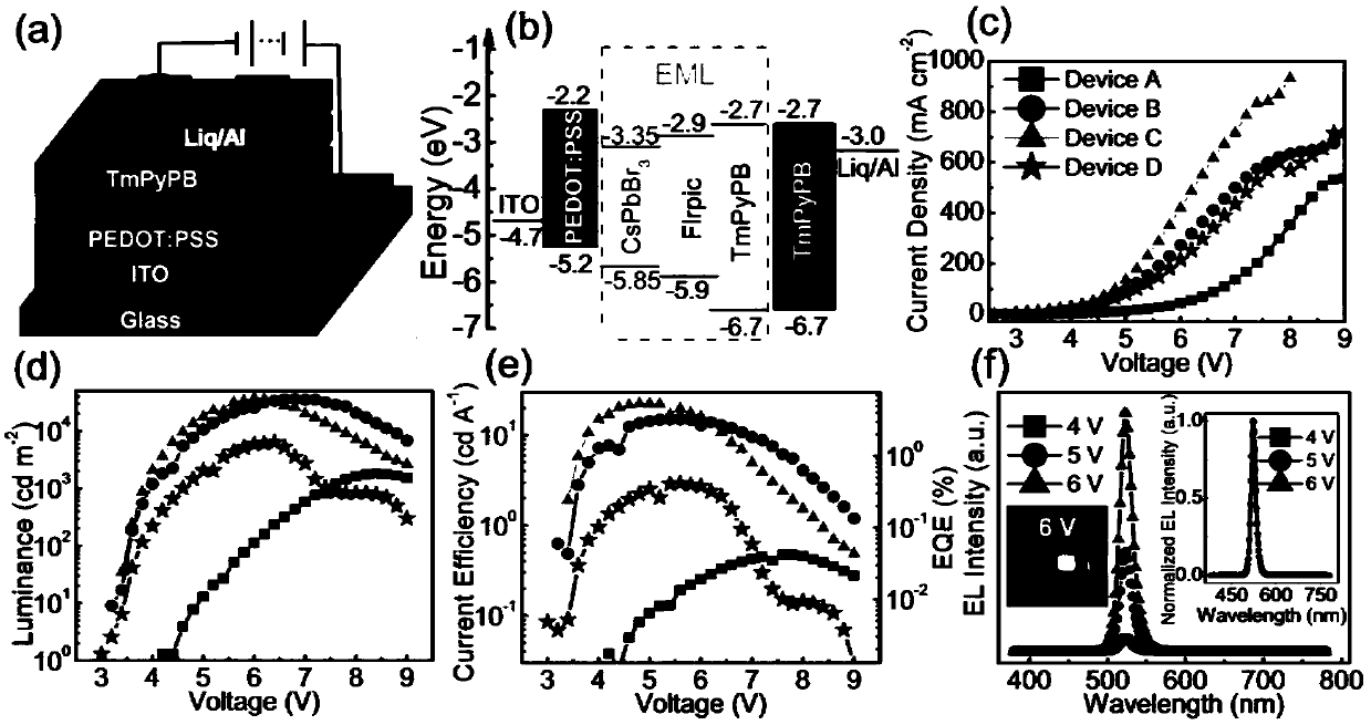
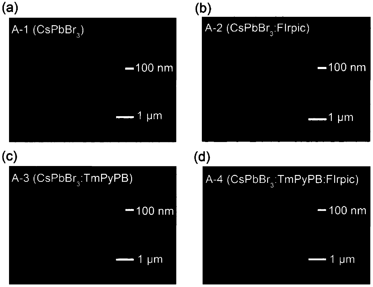
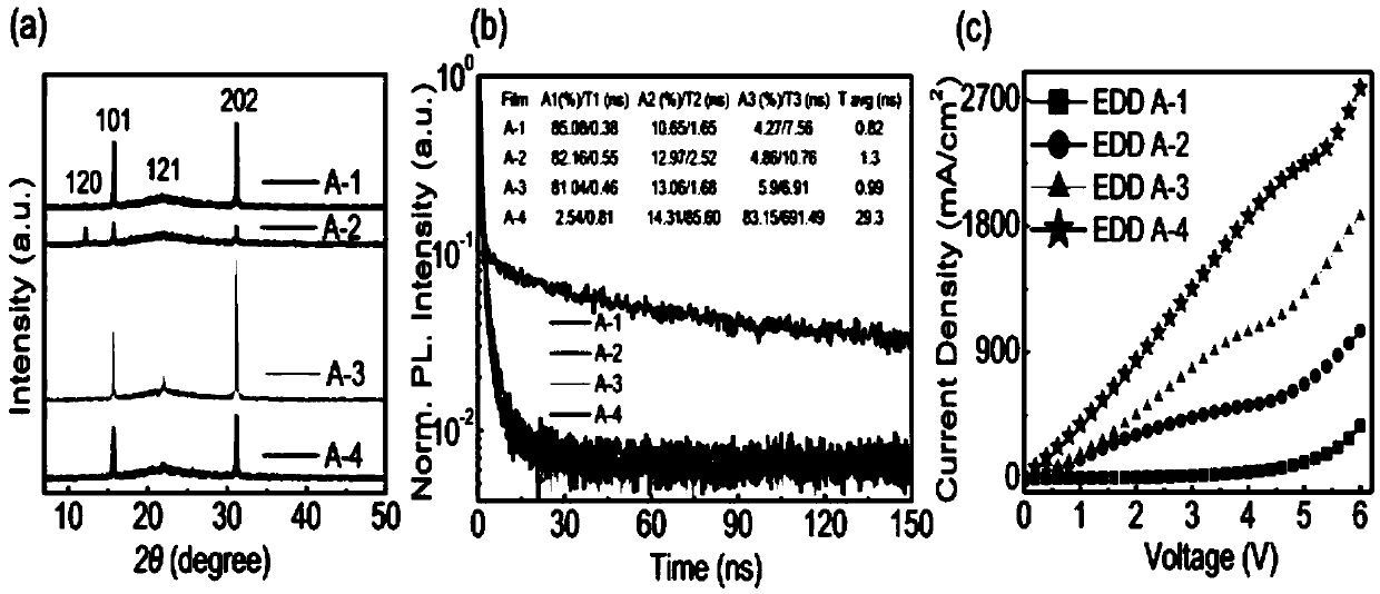
[0016] Preparation of perovskite solution: PbBr 2 (purchased from Alfa Aesar company, the purity is 99.999%) and CsBr (purchased from Alfa Aesar company, the purity is 99.999%) are dissolved in dimethyl sulfoxide solvent (purchased from Aladdin company, purity ≥ 99.8%) in order to prepare perovskite (CsPbBr 3 ) solution. 1,3,5-tri(m-pyrid-3-yl-phenyl)benzene (TmPyPB, purchased from Suzhou Fangsheng Optoelectronics Co., Ltd., purity>99.5%) and bis[(4,6-difluorophenyl)-pyridi- nato-N,C2'](picolinate)iridium...


PUM

PropertyMeasurementUnit
external quantum efficiencyaaaaaaaaaa

Abstract

The invention relates to a perovskite composite film, a light emitting diode and a preparation method of a perovskite composite film. The preparation method of a perovskite composite film prepares a flat and fully covered perovskite film by adding an electron transporting material and a phosphorescent sensitizer to an inorganic cerium halide perovskite CsPbBr3, prepares high-performance green light PeLEDs on the basis of taking the perovskite composite film as a light-emitting layer, improves the balance of carrier transport and increases the internal quantum efficiency so as to further increase the luminous efficiency and the service life of a perovskite light-emitting device.

Description

technical field [0001] The invention relates to the technical field of thin film preparation, in particular to a perovskite composite thin film and a preparation method, and to a light emitting diode with the composite thin film. Background technique [0002] Increasing research efforts have focused on low-cost and solution-processable metal halide perovskite materials due to their excellent optoelectronic properties in optoelectronic applications such as solar cells (SCs), photodetectors, lasers, and light-emitting diodes. characteristic. In particular, it has an electroluminescent spectrum with a narrow half-maximum width (FWHM) of about 20nm, tunable optical bandgap (from ultraviolet-to near-infrared), high photoluminescence quantum yield (PLQY), and high carrier Mobility (μ ~ 1 to 4500cm 2 V -1 the s -1 ) and low density of defect states, making them promising as light-emitting sources for perovskite light-emitting diodes (PeLEDs) in next-generation displays and ligh...

Claims


Application Information

Patent Timeline
Patent Type & Authority Applications(China)
IPC IPC(8): H01L51/50H01L51/54H01L51/56
CPCH10K50/121H10K50/165H10K2102/00H10K71/00
Inventor 高春红玉福星周东叶熊自阳马兴娟张月贾亚兰王润
Owner SOUTHWEST UNIVERSITY
Why Eureka
Try Eureka