Method for fabricating solar cell

A solar cell and manufacturing method technology, applied in circuits, photovoltaic power generation, electrical components, etc., can solve the problems of affecting the open voltage and conversion efficiency of solar cells, reducing the utilization rate of sunlight, serious light absorption, etc., to solve passivation and light absorption. , Improve open circuit voltage and conversion efficiency, reduce the effect of minority carrier recombination

Active Publication Date: 2018-11-16
KINGSTONE SEMICONDUCTOR LIMITED COMPANY
View PDF14 Cites 3 Cited by
  • Summary
  • Abstract
  • Description
  • Claims
  • Application Information

AI Technical Summary

Problems solved by technology

However, after this type of passivation layer is formed, the contact position between the metal and the silicon substrate will be relatively large, which affects the opening voltage and conversion efficiency of the solar cell.
[0003] For this reason, the industry proposes to use polysilicon materials instead of oxides or nitrides, but this has caused new problems. Polysilicon materials absorb light very seriously. The recombination of metal-semiconductor contact positions, but due to the serious light absorption of polysilicon, reduces the utilization rate of sunlight

Method used


Image

  • Method for fabricating solar cell
  • Method for fabricating solar cell
  • Method for fabricating solar cell

Examples


Embodiment 1

[0047] refer to Figure 1-Figure 6 , to introduce the manufacturing method of this embodiment.

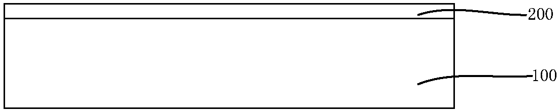
[0048] refer to figure 1 , forming an oxide layer 200 on the front surface of the substrate 100 of the first conductivity type, for example, an n-type silicon wafer.

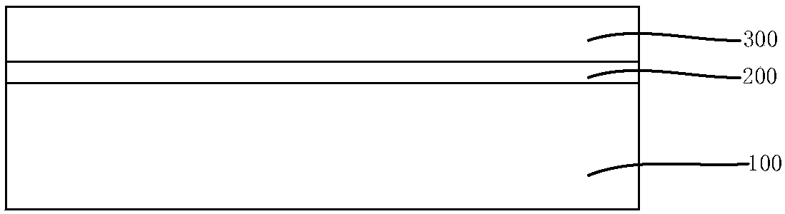
[0049] refer to figure 2 , forming amorphous silicon 300 on the oxide layer 200 .

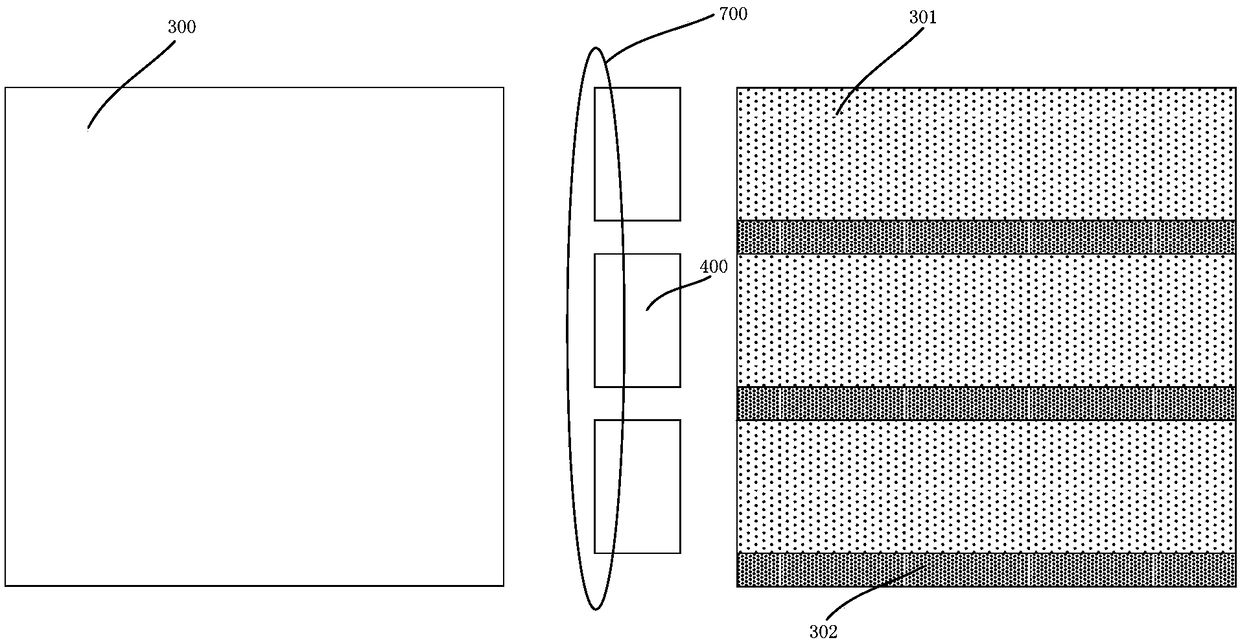
[0050] refer to image 3 with Figure 4 The amorphous silicon is selectively doped with a doping element of the second conductivity type to form a heavily doped region 302 and a lightly doped region 301 (both the heavily doped region and the lightly doped region are doped with the second conductivity type element. Miscellaneous), such as p-type doping, implanting boron ions. Specifically, a barrier layer 400 with a hollow area is set between the workpiece to be processed and the beam 700, and the beam and the barrier layer partially overlap, so that the workpiece (the workpiece here is figure 2 structure) moving from left to ...

Embodiment 2

[0054] The principle of embodiment 2 is the same as that of embodiment 1, the difference is:

[0055] refer to Figure 7-Figure 11 , before forming the oxide layer, a second conductivity type doped layer 600, such as a p-type doped layer, is firstly formed in the front surface of the first conductivity type substrate 100, such as an n-type silicon wafer. Doping can be achieved by existing means, such as boron diffusion or boron ion implantation. Then the oxide layer 200 is formed on the doped layer 600 of the second conductivity type.

[0056] refer to Figure 8-Figure 11 , polysilicon 300 is formed on the oxide layer 200, and then a heavily boron-doped region 302 and a lightly boron-doped region 302 are formed in the polysilicon through a barrier layer provided with a hollow area combined with ion implantation (implantation of a second conductivity type dopant element, such as boron element). impurity region 301, and heat-treat the ion-implanted structure.

[0057] The su...

Embodiment 3

[0059] The principle of embodiment 3 is the same as that of embodiment 2, the difference is:

[0060] refer to Figure 12 In this embodiment, only the heavily doped region 302 remains, the lightly doped polysilicon is completely etched away, and electrodes are formed on the heavily doped region. Refer to Example 2 for the remaining steps.

[0061] In the present invention, light and heavy doping of polysilicon can form a carrier selective electrode and reduce the recombination of metal and silicon contacts. Since the doped regions of different doses in polysilicon have different tolerances to alkaline reagents, selective etching can be formed, thereby forming thicker polysilicon under the metal contact, and forming thinner polysilicon in the light-receiving part. Thus, the contradiction between passivation and light absorption is solved.


PUM

PropertyMeasurementUnit
thicknessaaaaaaaaaa
thicknessaaaaaaaaaa
thicknessaaaaaaaaaa

Abstract

The invention discloses a method for fabricating a solar cell, comprising a step S1 of forming an oxide layer on the surface of a first conductive type of substrate; a step S2 of forming polycrystalline silicon or amorphous silicon on the oxide layer; a step S3 of selectively doping the polycrystalline silicon or amorphous silicon with a second conductive type of doping element to form a heavily doped region and a lightly doped region; a step S4 of subjecting the structure obtained in the step S3 to heat treatment in order to convert the amorphous silicon into the polycrystalline silicon; a step S5 of selectively etching the polycrystalline silicon obtained in the step S4 with an alkaline reagent; and a step S6 of forming an electrode in the heavily doped region. The method forms the metalon the thick polycrystalline silicon by selectively doping the polycrystalline silicon, thereby reducing the recombination at a metal and semiconductor contact position. Further, the thin polycrystalline silicon is used for light transmission so as to achieve a passivation effect and light transmission balance.

Description

technical field [0001] The invention relates to a method for manufacturing a solar cell, in particular to a method for manufacturing a solar cell with good passivation effect and light transmission effect. Background technique [0002] No matter what kind of solar cell, after the doping of the PN structure is completed and before metallization, surface passivation is required. Usually, the passivation layer can be realized by oxide or nitride. After forming the passivation layer, metal is deposited on the passivation layer and finally sintered, so that the metal and the silicon substrate come into contact. However, after this type of passivation layer forms electrodes, the recombination will be relatively large at the contact position between the metal and the silicon substrate, thereby affecting the opening voltage and conversion efficiency of the solar cell. [0003] For this reason, the industry proposes to use polysilicon materials instead of oxides or nitrides, but thi...

Claims


Application Information

Patent Timeline
Patent Type & Authority Applications(China)
IPC IPC(8): H01L31/18H01L31/068
CPCH01L31/068H01L31/1804H01L31/1868Y02E10/546Y02E10/547Y02P70/50
Inventor 何川金光耀陈炯
Owner KINGSTONE SEMICONDUCTOR LIMITED COMPANY
Why Eureka
Try Eureka