

Multilayer ceramic capacitor and preparation method thereof
A technology of multilayer ceramics and capacitors, which is applied in the direction of laminated capacitors, capacitors, fixed capacitors, etc., can solve the problems of incomplete removal of adhesives, decline in the density and uniformity of ceramic bodies, and achieve good consistency and high density. and good dielectric properties
- Summary
- Abstract
- Description
- Claims
- Application Information
AI Technical Summary
Problems solved by technology
Method used
Image

Examples
no. 1 approach
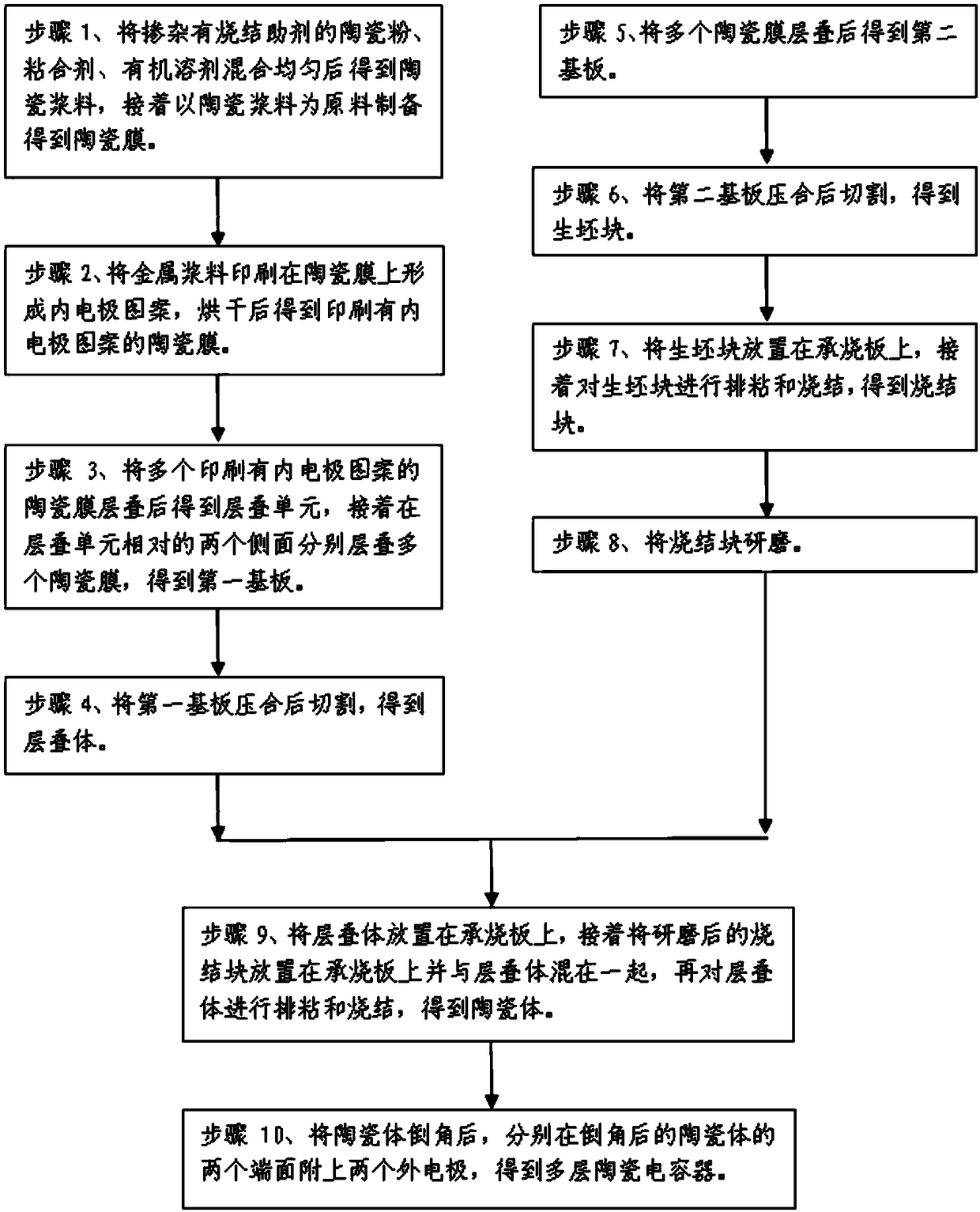
[0055] An embodiment of the multilayer ceramic capacitor of the present invention, combined with figure 1 , the multilayer ceramic capacitor described in this embodiment is prepared by the following method:
[0056] Step 1: Mix ceramic powder doped with sintering aid, binder, and organic solvent uniformly to obtain a ceramic slurry, and then use the ceramic slurry as a raw material to prepare a ceramic film.
[0057] In this embodiment, the operation of uniformly mixing the ceramic powder doped with sintering aid, the binder, and the organic solvent is as follows: the ceramic powder doped with the sintering aid, the adhesive, and the organic solvent are uniformly mixed by ball milling , The ball milling time can be 10~16h.
[0058] In the ceramic slurry, the mass ratio of the ceramic powder doped with the sintering aid, the binder and the organic solvent is 10:(3-5):(6-9).
[0059] In this embodiment, in the ceramic powder doped with the sintering aid, the mass percentage of...
no. 2 approach
[0099] An embodiment of the multilayer ceramic capacitor of the present invention, the multilayer ceramic capacitor described in this embodiment is prepared by the following method:
[0100] Steps 1 to 6 are the same as those in the first embodiment.
[0101] Step 7: Grinding the green block.
[0102] Using alumina balls or zirconia balls, and tap water as the grinding medium, the green body is ground by planetary grinding or barrel grinding, so that the six sides of the green body are ground into concave surfaces. The ground green body block is generally rectangular and has six inwardly concave faces.
[0103] The green body block has certain plasticity and relatively small hardness, and it will not be broken when it is ground, and it is relatively easy to grind it to the degree of surface depression, and the grinding efficiency is high.
[0104] Step 8: placing the ground green body on the setter, and then debonding and sintering the green body to obtain a sintered block. ...
no. 3 approach
[0112] Steps 1 to 4 are the same as those in the first embodiment.
[0113] Step 5: Printing nickel paste on the ceramic film obtained in step 1 to form an additional layer, and stacking a plurality of ceramic films printed with the additional layer to obtain a second substrate.
[0114] In the operation of printing nickel paste on the ceramic film to form an additional layer, the screen printing process is selected for printing. The thickness of the additional layer may be 2-5 μm.
[0115] Generally, the second substrate can be obtained by laminating 6 to 38 ceramic membranes printed with additional layers.
[0116] Steps 6 to 10 are the same as those in the first embodiment. The side view of the sintered block in this embodiment is as Figure 6 As shown, the side view of the ground sintered block is shown in Figure 7 It should be noted that since the sintered block of the present embodiment contains nickel, the ceramic body can be more conveniently separated from the si...
PUM
| Property | Measurement | Unit |
|---|---|---|
| Thickness | aaaaa | aaaaa |
Abstract
Description
Claims
Application Information