Preparation method and application for patterned two-dimensional conjugate microporous polymer

A microporous polymer and two-dimensional conjugation technology, applied in the field of polymer semiconductor materials, can solve the problems of mold shrinkage deformation, expensive, film damage, etc., and achieve the effect of mild reaction conditions, easy industrial application, and easy transfer

Active Publication Date: 2018-11-30
NANJING UNIV OF TECH
View PDF4 Cites 5 Cited by
  • Summary
  • Abstract
  • Description
  • Claims
  • Application Information

AI Technical Summary

Problems solved by technology
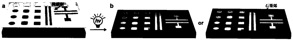
However, these methods are difficult to prepare large-area polymer films, and these methods are relatively complicated
At the same time, it is an important step to prepare patterning on the polymer film for its application in optoelectronic devices. At present, the methods for preparing patterning mainly include interface assembly, photolithography, soft etching, and imprinting [Advanced Materials, 2009, 21,...

Method used


Image

  • Preparation method and application for patterned two-dimensional conjugate microporous polymer
  • Preparation method and application for patterned two-dimensional conjugate microporous polymer
  • Preparation method and application for patterned two-dimensional conjugate microporous polymer

Examples


Embodiment 1

[0054] Preparation of poly 9,9'-biscarbazole (Material I)

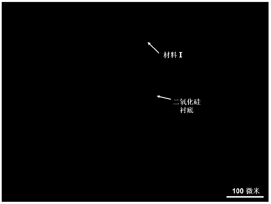
[0055] A schematic diagram of the polymerization process is shown in figure 1 As shown, the specific steps are as follows: the chlorobenzene solution of 10mg / mL 9,9'-biscarbazole is spin-coated on a clean silicon dioxide (300 nm) / silicon wafer substrate, and the spin-coating condition is 4000 rpm minutes, 20 seconds. The monomer-spin-coated substrate was then dried in an oven at 120 °C for 30 minutes, and the mask was placed on the monomer-spin-coated substrate. Then, under the condition of 25°C, place the substrate under the light source, take it out after reacting for 1 hour, then remove the mask plate, and wash the sample repeatedly with dichloromethane and ethanol in sequence. After drying in an oven at 50 °C, a large-area, patterned ultrathin poly-9,9'-biscarbazole film grown on the substrate was obtained. It was found by optical microscopy that patterned two-dimensional conjugated microporous polymers ( fig...

Embodiment 2

[0057] Preparation of poly 4,4'-bis(N-carbazole)-1,1'-biphenyl (material Ⅲ)

[0058] Spin-coat a 10 mg / mL solution of 4,4'-bis(N-carbazole)-1,1'-biphenyl in chlorobenzene on a clean silica (300 nm) / silicon wafer substrate, spin-coat The conditions are 4000 rpm, 20 seconds. The monomer-spin-coated substrate was then dried in an oven at 120° C. for 30 minutes, and a mask was placed on the substrate. Then, under the condition of 25°C, place the substrate under the light source, take it out after reacting for 1 hour, then remove the mask plate, and wash the sample repeatedly with dichloromethane and ethanol in sequence. After drying in an oven at 50°C, a large-area, patterned ultrathin poly 4,4'-bis(N-carbazole)-1,1'-biphenyl film grown on the substrate was obtained.

[0059] The prepared materials were photographed, and it can be seen from the figure that we can prepare two-dimensional conjugated microporous polymers with different patterns by using different masks, including c...

Embodiment 3

[0065] Preparation of poly 4,4'-bis(N-carbazole)thiophene (Material Ⅳ)

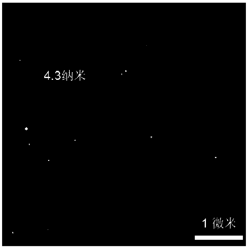
[0066] Spin-coat a 10 mg / mL chlorobenzene solution of 4,4'-bis(N-carbazole)thiophene on a clean silica (300 nm) / silicon wafer substrate at 4000 rpm, 20 seconds. The monomer-spin-coated substrate was then dried in an oven at 120°C for 30 minutes, and a mask was placed on the substrate. Then, under the condition of 25°C, place the substrate under the light source, take it out after reacting for 1 hour, then remove the mask plate, and wash the sample repeatedly with dichloromethane and ethanol successively. After drying in an oven at 50 °C, large-area, patterned ultrathin poly-4,4'-bis(N-carbazole)thiophene films grown on substrates were obtained. It was found by optical microscopy that patterned two-dimensional conjugated microporous polymers ( Figure 11 ). The thickness of the obtained polymer film measured by atomic force microscope is about 3.7 nanometers ( Figure 12 ).


PUM

PropertyMeasurementUnit
Thicknessaaaaaaaaaa
Thicknessaaaaaaaaaa
Thicknessaaaaaaaaaa

Abstract

The invention discloses a preparation method and application for a patterned two-dimensional conjugate microporous polymer, and belongs to the field of polymer semiconductor materials. The two-dimensional conjugate microporous polymer uses carbazole as a skeleton; and the preparation method comprises the followings steps: rotatingly coating a flat substrate by a carbazole derivative or dripping the carbazole derivative on the flat substrate to form a film, adding a mask to the monomer film, placing the treated film under a light source, performing a photopolymerization reaction, wherein the irradiated monomer is subjected to a cross-linking reaction, and the monomer masked by the mask is not subjected to a reaction, and soaking the irradiated monomer film in an organic solvent, wherein thefilm subjected to the cross-linking reaction generates a polymer, and the unreacted monomer is dissolved, so that the large-area patterned ultra-thin two-dimensional conjugate microporous polymer film is prepared. The method disclosed by the invention is a direct patterning method, and avoids the steps of etching and the like in a conventional patterning method; and the patterned film can be applied to devices without transfer.

Description

technical field [0001] The invention belongs to the field of polymer semiconductor materials, and specifically relates to a large-area, patterned ultrathin two-dimensional conjugated microporous polymer semiconductor material and its preparation method and application. Background technique [0002] Since the discovery of conductive polyethylene in 1977, a large number of conjugated polymers (CPs) have been synthesized and widely used in various fields [Journal of Materials Chemistry, 2007, 17, 4289-4296]. As a class of conjugated polymers with special microporous structure, they are called two-dimensional conjugated microporous polymers. Two-dimensional conjugated microporous polymers have attracted the attention of scientific researchers due to their unique π-extended conjugated system and inherent microporous 3D skeleton structure. Their high specific surface area, diverse preparation methods, chemical stability, and thermal stability It is mainly used in the fields of ad...

Claims


Application Information

Patent Timeline
IPC IPC(8): C08G73/06
CPCC08G73/0688
Inventor 刘举庆尹宇航刘正东黄维
Owner NANJING UNIV OF TECH
Why Eureka
Try Eureka