Luminescent device and manufacturing method thereof

A manufacturing method and technology for light-emitting devices, applied in semiconductor devices, electrical components, circuits, etc., can solve the problems of increasing the number of manufacturing processes, declining performance of light-emitting devices, and low product competitiveness, reducing the number of process processes and eliminating solvents. The effect of poor vapor concentration and shortening of the printing process

Active Publication Date: 2018-12-07
GUANGDONG JUHUA PRINTING DISPLAY TECH CO LTD
View PDF4 Cites 9 Cited by
  • Summary
  • Abstract
  • Description
  • Claims
  • Application Information

AI Technical Summary

Problems solved by technology

[0004] (1) Make the overall drying process complicated and inefficient
This is because most light-emitting devices require multiple printing processes of inks with different functional materials, which also require multiple printing processes of vacuum drying and vacuum breaking, which obviously increases the number of production processes.
[0005] (2) The process of one-time vacuum drying after one-time printing is easy to cause uneven film formation in the production of medium and large display panels
This is because there is likely to be a large vapor pressure difference above the large-scale printed pattern, which leads to the extremely uneven film formation of pixels at the edge of the pattern and the formation of mura (color halo)
This not only leads to a decrease in the performance of the light-emitting device, but also makes the product less competitive

Method used


Image

  • Luminescent device and manufacturing method thereof
  • Luminescent device and manufacturing method thereof
  • Luminescent device and manufacturing method thereof

Examples


Embodiment 1

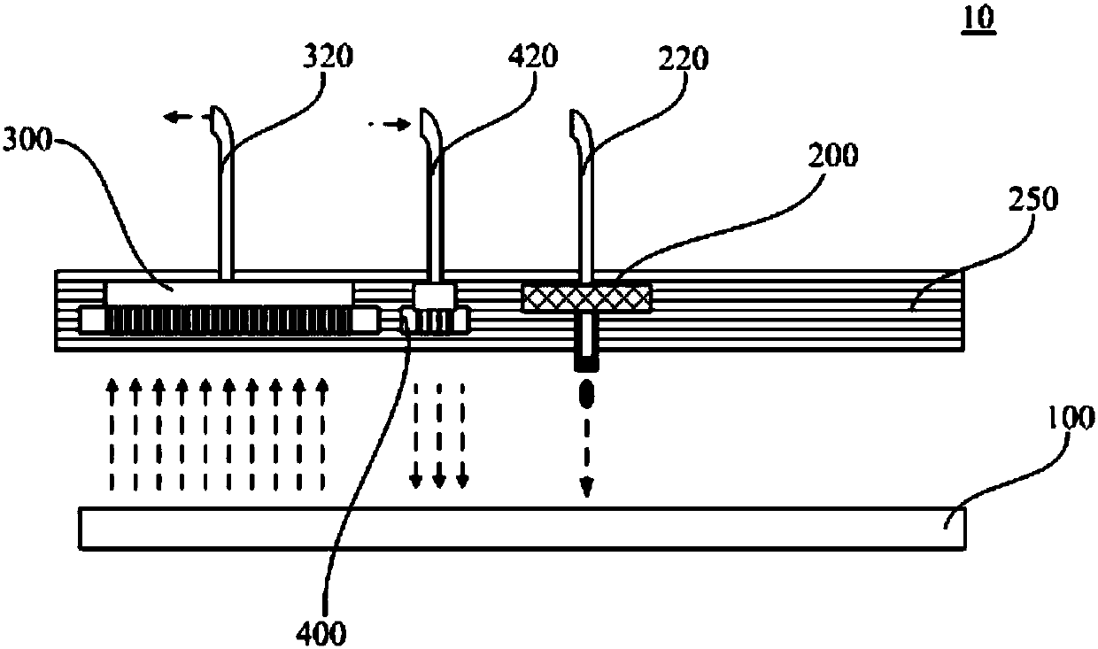
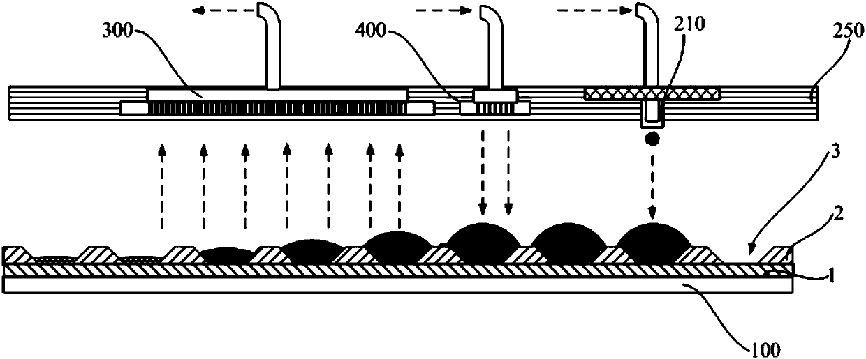
[0113] This embodiment provides a method for manufacturing a printed display, which includes the following steps:

[0114] 1) Prepare a pixel defining layer 2 on a patterned anode TFT substrate 1, and form a pixel pit 3.

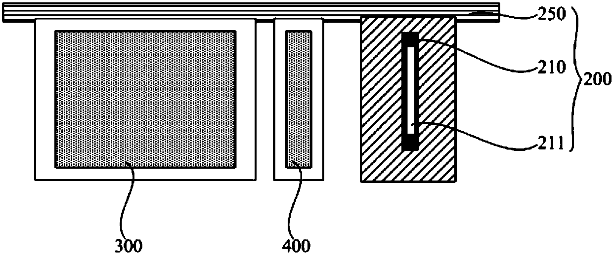
[0115] 2), please further combine image 3 , using the printing device 10 to ink-jet print functional ink into the pixel pit 3, and perform step-by-step vacuum drying treatment on the printed ink to obtain a pre-dried film.

[0116] 3) heat-treating the pre-dried film to make it completely cross-linked and cured to form a light-emitting functional layer.

[0117] Wherein, the light-emitting functional layer includes a hole injection layer, a hole transport layer, and a light-emitting layer, and the formation process of each layer adopts a step-by-step vacuum drying process while inkjet printing is performed.

[0118] 4), evaporating the electron transport layer and the cathode, and finally packaging, that is.

[0119] This embodiment provides a method for...


PUM


Abstract

The present invention relates to a luminescent device and manufacturing method thereof. The manufacturing method comprises the following steps of: providing a substrate, and forming a first electrodelayer on the substrate; forming a pixel pit on the substrate; forming a luminescent function layer in the pixel pit; forming a second electrode layer on a pixel definition layer and the luminescent function layer, wherein the formation process of at least one layer of the first electrode layer, the second electrode layer and the luminescent function layer comprises the following steps of: performing ink-jet printing, at the same time performing step-by-step vacuum drying processing of ink after printing, performing package and obtaining at least one layer of the first electrode layer, the second electrode layer and the luminescent function layer. The manufacturing method of the luminescent device facilitates improvement of the uniformity of final film formation, greatly shortens the wholeprinting craft process, reduces the craft flow numbers and improves the printing production efficiency.

Description

technical field [0001] The invention relates to the field of display devices, in particular to a light emitting device and a manufacturing method thereof. Background technique [0002] With the gradual development of display technology, light-emitting devices such as OLEDs have attracted the attention of all parties due to their excellent display performance. Conventional evaporation methods to manufacture OLEDs and other light-emitting devices face problems such as low material utilization and the need for ultra-fine masks, resulting in high production costs. In order to further reduce the production cost of OLEDs and other light-emitting devices, printing technology can be used to manufacture OLEDs and other light-emitting devices. [0003] One of the key problems in the production of OLED and other light-emitting devices by printing technology is the drying and film-forming process after inkjet printing of functional material inks. The drying and film-forming process dir...

Claims


Application Information

Patent Timeline
Patent Type & Authority Applications(China)
IPC IPC(8): H01L33/48H01L33/64
CPCH01L33/486H01L33/642
Inventor 董婷
Owner GUANGDONG JUHUA PRINTING DISPLAY TECH CO LTD
Why Eureka
Try Eureka