Synaptic device based on metal cation modified black phosphorus and preparation method thereof
A technology of metal cations and synaptic devices, which is applied in the field of artificial neural networks, can solve the problems of further improvement in related performance and fewer devices, and achieve excellent synaptic performance, simple and easy operation, and good environmental stability.
- Summary
- Abstract
- Description
- Claims
- Application Information
AI Technical Summary
Problems solved by technology
Method used
Image
Examples
preparation example Construction
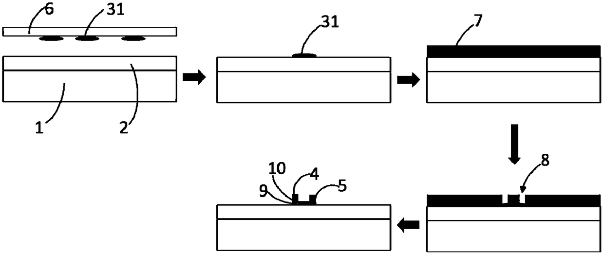
[0049] Please refer to figure 2 , the second aspect of the embodiment of the present invention provides a method for preparing a synaptic device based on metal cation-modified black phosphorus, including:
[0050] S01, providing a back gate electrode 1 and an isolation layer 2 disposed on the back gate electrode 1;
[0051] S02, transferring the black phosphorus flakes 31 onto the isolation layer 2;
[0052] S03. Spin-coat photoresist 7 over the black phosphorus flake 31 and the isolation layer 2 not covered by the black phosphorus flake 31, and form an electrode pattern 8 after exposure and development;
[0053] S04, depositing the electrode material, and then stripping off the photoresist to form the first electrode 4 and the second electrode 5 to obtain the synaptic device;
[0054] S05. Soak the synaptic device in a solution containing metal cations for 0.2-2 hours, take it out and dry it, and obtain a synaptic device based on metal cation-modified black phosphorus.
...
Embodiment 1
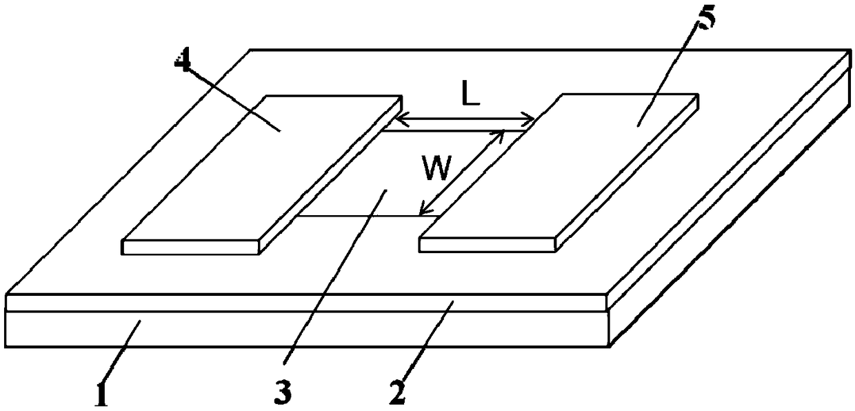
[0067] as attached figure 1 As shown, the present invention provides a synaptic device based on silver ion-modified black phosphorus. The device has a field effect tube structure, and the functional layer is a silver-ion-modified black phosphorus sheet. The device has a p-type or n-type doped silicon layer 1 , a silicon dioxide layer 2 , a silver ion-modified black phosphorus sheet 3 , a first electrode 4 and a second electrode 5 sequentially from bottom to top. The silicon layer has a thickness of 300 μm and a resistivity of 1-10 Ω·cm. The silicon dioxide layer has a thickness of 300 nm. The thickness of the black phosphorus flakes decorated with silver ions is 20nm. Both the first electrode and the second electrode are chromium / gold material, wherein the thickness of the chromium layer is 5nm, and the thickness of the gold layer is 40nm. That is, the first electrode and the second electrode are composite electrodes formed by stacking a chromium layer with a thickness of 5...
Embodiment 2
[0079] as attached figure 1As shown, the present invention provides a synaptic device based on iron ion-modified black phosphorus. The device has a field effect tube structure, and the functional layer is a black phosphorus sheet modified by iron ion. The device has a p-type or n-type doped silicon layer 1 , a silicon dioxide layer 2 , an iron ion-modified black phosphorus sheet 3 , a first electrode 4 and a second electrode 5 in sequence from bottom to top. The silicon layer has a thickness of 500 μm and a resistivity of 1-10 Ω·cm. The silicon dioxide layer has a thickness of 300 nm. The thickness of the black phosphorus flakes decorated with iron ions is 20nm. Both the first electrode and the second electrode are made of chromium / gold, wherein the thickness of chromium is 5nm, and the thickness of gold is 40nm. That is, the first electrode and the second electrode are composite electrodes formed by stacking a chromium layer with a thickness of 5 nm and a gold layer with a...
PUM
 Abstract
Description
Claims
Application Information


