A novel photodetector based on perovskite and a manufacturing method thereof

A technology of photodetector and manufacturing method, which is applied in the field of photoelectric detection, and can solve the problems of low probability of interlayer transmission, poor air stability, low driving voltage, etc.

Active Publication Date: 2018-12-18
SHANGHAI INTEGRATED CIRCUIT RES & DEV CENT +1
View PDF8 Cites 7 Cited by
  • Summary
  • Abstract
  • Description
  • Claims
  • Application Information

AI Technical Summary

Problems solved by technology

[0002] At present, perovskite materials are more and more widely used in the field of photoelectric detection. The more commonly used perovskites include perovskites with two-dimensional or three-dimensional structures. Two-dimensional perovskites have a special two-dimensional planar structure. It has good room temperature stability, and the two-dimensional perovskite has low driving voltage and high-efficiency exciton separation characteristics, making it of high value in the field of photodetection, but the carriers in the two-dimensional perovskite The transmission is more inclined to intralayer transmission, and the probability of interlayer transmission is lower, making two-dimensional perovskites more commonly used in photodetectors with horizontal structures; compared with two-dimensional perovskites, carriers in three-dimensional perovskites The transport in is more inclined to interlayer transport, and the three-dimensional perovskite has a high photoelectric conversion efficiency, but the air stability of the three-dimensional perovskite is poor

Method used


Image

  • A novel photodetector based on perovskite and a manufacturing method thereof
  • A novel photodetector based on perovskite and a manufacturing method thereof
  • A novel photodetector based on perovskite and a manufacturing method thereof

Examples


Embodiment Construction

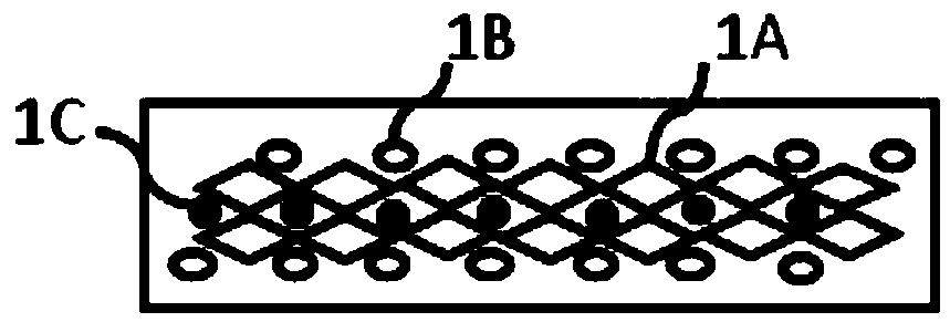
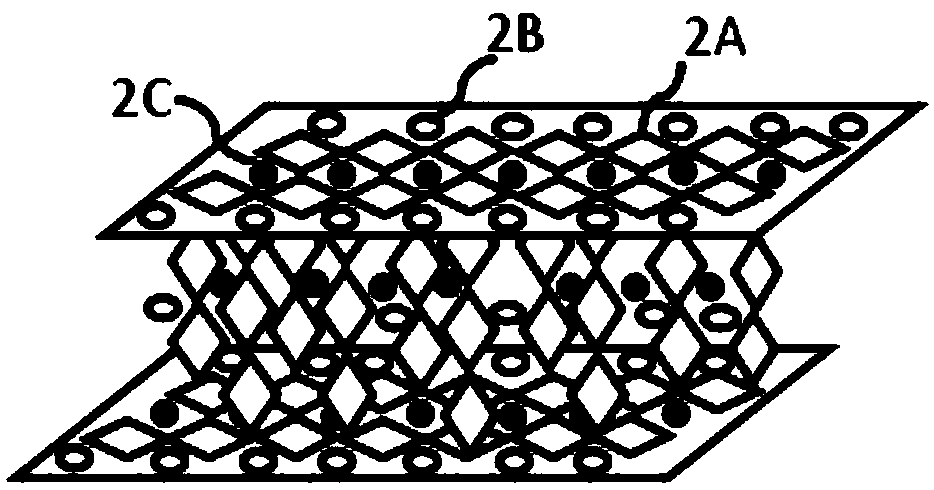
[0048] In order to make the purpose, advantages and characteristics of the present invention clearer, the following in conjunction with the attached Figure 1-20 The novel photodetector based on perovskite proposed by the present invention and its manufacturing method are further described in detail. It should be noted that all the drawings are in a very simplified form and use imprecise scales, and are only used to facilitate and clearly assist the purpose of illustrating the embodiments of the present invention.

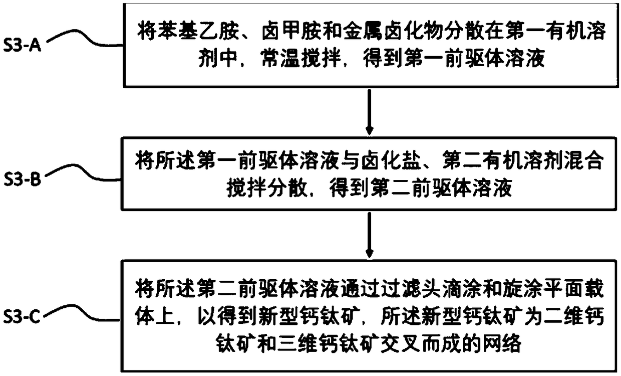
[0049] An embodiment of the present invention provides a method for making a novel perovskite, see image 3 , image 3 It is a flowchart of a method for producing a novel perovskite according to an embodiment of the present invention, and the method for producing a novel perovskite includes:

[0050] Step S3-A, dispersing phenylethylamine, halomethylamine and metal halide in the first organic solvent, stirring at room temperature, to obtain the first precursor solu...


PUM


Abstract

The invention provides a novel photodetector based on perovskite and a manufacturing method thereof. A novel photodetector with a vertical structure is fabricated by sequentially arranging a first electrode, a hole transport layer, a photosensitive active layer containing perovskite, an electron transport layer and a second electrode on the substrate from bottom to top. The photosensitive active layer is a novel perovskite with a two-dimensional perovskite and a three-dimensional perovskite cross network structure produced by adding a halide salt and an organic solvent into a two-dimensional perovskite precursor solution. The two-dimensional perovskite and the three-dimensional perovskite cross network structure increase the crystallinity of the novel perovskite, Carrie lifetime prolongation, Moreover, the novel perovskite possesses the characteristics of both in-plane and inter-plane transport of carriers, and the novel photodetector containing the novel perovskite possesses larger photocurrent and higher photoresponse, and exhibits excellent air stability and long-term cycling stability.

Description

technical field [0001] The invention relates to the field of photoelectric detection, in particular to a novel photodetector based on perovskite and a manufacturing method thereof. Background technique [0002] At present, perovskite materials are more and more widely used in the field of photoelectric detection. The more commonly used perovskites include perovskites with two-dimensional or three-dimensional structures. Two-dimensional perovskites have a special two-dimensional planar structure. It has good room temperature stability, and the two-dimensional perovskite has low driving voltage and efficient exciton separation characteristics, making it of high value in the field of photodetection, but the carriers in the two-dimensional perovskite The transmission is more inclined to intralayer transmission, and the probability of interlayer transmission is lower, making two-dimensional perovskites more commonly used in photodetectors with horizontal structures; compared with...

Claims


Application Information

Patent Timeline
Patent Type & Authority Applications(China)
IPC IPC(8): H01L51/48H01L51/42
CPCH10K71/12H10K30/30Y02E10/549Y02P70/50
Inventor 武青青严亚杰梁子骐朱建军胡少坚
Owner SHANGHAI INTEGRATED CIRCUIT RES & DEV CENT
Why Eureka
Try Eureka