SPR nerve synaptic device based on a-Si memristor effect and preparation method thereof

A technology of neural synapse and memristor, which is applied in the field of bionic devices, can solve the problems of small signal processing bandwidth and signal transmission crosstalk, and achieve the effect of large signal processing bandwidth, large bandwidth, and avoiding grazing incidence

Active Publication Date: 2018-12-21
UNIV OF ELECTRONICS SCI & TECH OF CHINA
View PDF9 Cites 5 Cited by
  • Summary
  • Abstract
  • Description
  • Claims
  • Application Information

AI Technical Summary

Problems solved by technology

[0004] In view of the above, the present invention provides an optical sensor based on the a-Si memristive effect for the problems of small signal processing bandwidth and prone to crosstalk in the signal transmission process existing in the existing memristor-based bionic synapse. Read SPR neural synaptic device and its preparation method

Method used


Image

  • SPR nerve synaptic device based on a-Si memristor effect and preparation method thereof
  • SPR nerve synaptic device based on a-Si memristor effect and preparation method thereof
  • SPR nerve synaptic device based on a-Si memristor effect and preparation method thereof

Examples


Embodiment 1

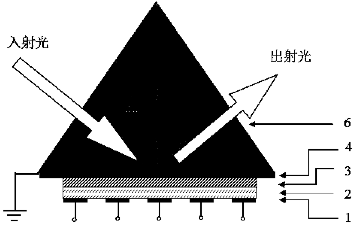
[0035] A SPR neurosynaptic device based on a-Si memristive effect, its structure is as follows figure 1 Shown: include a memristor and a crystalline silicon prism 6 arranged above the memristor. In this embodiment, the crystalline silicon prism 6 is a triangular prism processed from crystalline silicon. The memristor has "Bottom electrode 1 / first a-Si resistive layer 2 / second a-Si resistive layer 3 / top electrode 4" vertical four-layer structure, in this embodiment the top electrode 4 is deposited on the bottom surface of the crystalline silicon prism 6 Metal silver Ag, the second a-Si resistive layer 3 is an a-Si thin film containing Ag nanoparticles, the volume fraction of Ag nanoparticles is 40%, and the first a-Si resistive layer 2 is an a-Si film containing Ag nanoparticles a-Si film, the volume fraction of Ag nanoparticles is 5%, the top electrode 4 is metal platinum Pt deposited on the bottom surface of the first a-Si resistive layer 2; the refractive index of the crysta...

Embodiment 2

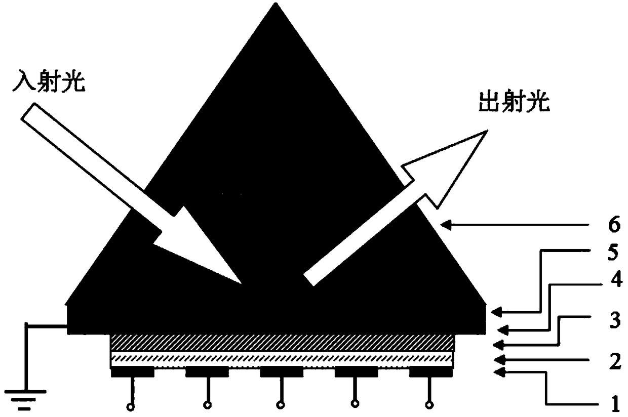
[0044] A SPR neurosynaptic device based on a-Si memristive effect, its structure is as follows figure 1 Shown: comprise memristor and be arranged on the crystalline silicon wafer 5 above described memristor and be arranged on the crystalline silicon prism 6 above described crystalline silicon wafer 5, in the present embodiment, crystalline silicon prism 6 is processed by crystalline silicon The formed triangular prism, the crystalline silicon wafer 5 is also processed from crystalline silicon, and the crystalline silicon wafer 5 and the crystalline silicon prism 6 are preferably bonded with a refractive index matching liquid, and the memristor has a bottom-to-top Electrode 1 / first a-Si resistive layer 2 / second a-Si resistive layer 3 / top electrode 4" vertical four-layer structure, top electrode 4 in this embodiment is deposited on the bottom surface of crystalline silicon prism 6 Metal silver Ag, the second a-Si resistive switch layer 3 is an a-Si thin film containing Ag nanopa...


PUM

PropertyMeasurementUnit
thicknessaaaaaaaaaa
thicknessaaaaaaaaaa
wavelengthaaaaaaaaaa

Abstract

The invention relates to a SPR nerve synaptic device based on a-Si memristor effect and a preparation method thereof, belonging to the technical field of biomimetic devices. The invention combines thecrystalline silicon prism with the top electrode / a-Si: metal nanoparticle double resistive layer / bottom electrode memristor structure coupling, thereby making the optical signal modulated by the crystal silicon prism into the double resistive layer. A surface plasmon resonance (SPR) effect is utilize to read the dielectric constant change information of the resistive layer dure the working process of the device by the optical signal, thereby realizing the optical read of the synaptic weight of the device. The electrically modulated and optically read synaptic device of the invention has the advantages that the traditional electrically modulated and electrically read synaptic device cannot be compared with, because the synaptic device not only has the characteristics of low energy consumption and non-volatility of the traditional memristor, but also has the advantages of large signal processing bandwidth and strong electromagnetic interference resistance when the light is used as an information carrier.

Description

technical field [0001] The invention belongs to the technical field of bionic devices, and in particular relates to a SPR synapse device based on a-Si memristive effect and a preparation method thereof. Background technique [0002] Traditional computers are based on the "Von Neumann Architecture". However, in the "Von Neumann Architecture", the data call and transmission between the information memory and the processor are connected through the bus, which makes the efficiency of information processing It is not only affected by the computing speed and storage speed of the processor, but also restricted by the information transmission capacity of the bus, forming the so-called "Von Neumann bottleneck". Although the amount of information processed by the human brain is not less than that of a computer, it is obviously more efficient and consumes less energy. To this end, researchers have constructed the concept of an intelligent computer, expecting the computer to learn neur...

Claims


Application Information

Patent Timeline
Patent Type & Authority Applications(China)
IPC IPC(8): H01L45/00
CPCH10N70/257H10N70/011
Inventor 李伟陈奕丞次会聚董湘刘诚李东阳蒋向东
Owner UNIV OF ELECTRONICS SCI & TECH OF CHINA
Why Eureka
Try Eureka