Femtosecond laser preparation system and method for silicon photonic crystal waveguide device

A waveguide device and femtosecond laser technology, applied in the field of femtosecond laser preparation systems, can solve the problems of slow speed and low precision, and achieve the effects of ensuring accuracy, realizing high-precision processing and improving processing efficiency

Active Publication Date: 2020-04-24
HUBEI UNIV OF TECH
View PDF9 Cites 4 Cited by
  • Summary
  • Abstract
  • Description
  • Claims
  • Application Information

AI Technical Summary

Problems solved by technology

[0004] In order to overcome the problems of low precision and slow speed in the process of processing photonic crystal waveguides in the above-mentioned traditional methods, the present invention provides a femtosecond laser preparation system and method for silicon photonic crystal waveguides based on spatial light modulators, which can effectively improve Processing speed and processing accuracy

Method used


Image

  • Femtosecond laser preparation system and method for silicon photonic crystal waveguide device
  • Femtosecond laser preparation system and method for silicon photonic crystal waveguide device
  • Femtosecond laser preparation system and method for silicon photonic crystal waveguide device

Examples


Embodiment Construction

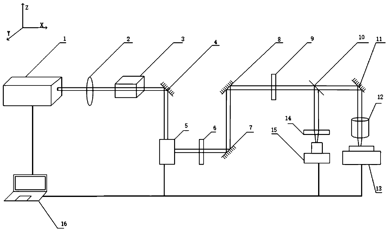
[0025] In order to facilitate those of ordinary skill in the art to understand and implement the present invention, the present invention will be described in further detail below in conjunction with the accompanying drawings and embodiments. It should be understood that the implementation examples described here are only used to illustrate and explain the present invention, and are not intended to limit this invention.

[0026] please see figure 1 A femtosecond laser preparation system for a silicon photonic crystal waveguide device provided by the present invention includes a femtosecond laser 1, a multi-stage half-wave plate 2, a polarization beam splitter prism 3, a first mirror 4, a spatial light modulator 5, a second A lens 6, a second mirror 7, a third mirror 8, a second lens 9, an electric flip mirror 10, a fourth mirror 11, a high-magnification objective lens 12, a three-dimensional processing platform 13, a third lens 14, a CCD camera 15, computer 16;

[0027] The ...


PUM

PropertyMeasurementUnit
diameteraaaaaaaaaa
thicknessaaaaaaaaaa
diameteraaaaaaaaaa

Abstract

The invention discloses a femtosecond laser preparation system and method for a silicon photonic crystal waveguide device. The femtosecond laser preparation system for the silicon photonic crystal waveguide device comprises a femtosecond laser, a multistage half-wave plate, a polarization splitting prism, a first reflecting mirror, a spatial light modulator, a first lens, a second reflecting mirror, a third reflecting mirror, a second lens, an electric flip mirror, a fourth reflecting mirror, a high-power objective lens, a three-dimensional processing platform, a third lens, a CCD camera and acomputer. Lasers output by the femtosecond laser pass through the multistage half-wave plate and the polarization splitting prism and pass through the reflecting mirrors to shoot into the spatial light modulator. A processing scheme is generated to a hologram by the computer, and the hologram is loaded to the spatial light modulator. After modulation is completed, light beams pass through the first lens, the second reflecting mirror, the third reflecting mirror, the second lens and the fourth reflecting mirror, and then are focused on a silicon substrate through the high-power objective lens,the movement of the three-dimensional processing platform is controlled by a program input into the computer to complete the processing task. The femtosecond laser preparation system and method for the silicon photonic crystal waveguide device has simple processing steps, high processing accuracy, high processing speed and low processing cost.

Description

technical field [0001] The invention belongs to the field of laser micromachining, and relates to a femtosecond laser preparation system and method for a silicon photonic crystal waveguide device, in particular to a femtosecond laser preparation system and method for a silicon photonic crystal waveguide device based on a spatial light modulator. Background technique [0002] The light guiding mechanism of the traditional dielectric optical waveguide is based on the principle of total reflection of light, and the ability to bind light is very weak. Even if the waveguide is only bent at 5°, the general optical field has more than 50% radiation loss. Therefore, bending Loss is a very serious problem faced by the development of traditional dielectric optical waveguides, and has become the bottleneck of its development; photonic crystals are artificial microstructures formed by periodically arranging substances with different dielectric constants in space. Line defects are introd...

Claims


Application Information

Patent Timeline
Patent Type & Authority Patents(China)
IPC IPC(8): G02B6/00B23K26/064B23K26/362B23K26/70
CPCB23K26/064B23K26/361B23K26/70
Inventor 陶青陈克楠刘顿陈列娄德元杨奇彪翟中生郑重
Owner HUBEI UNIV OF TECH
Why Eureka
Try Eureka