A LTCC substrate three-dimensional stacking structure and a hermetic packaging method thereof

A three-dimensional stacking and hermetic packaging technology, which is applied in the direction of electrical components, electrical solid devices, circuits, etc., can solve the problems of inability to achieve airtightness, complicated process, and many welding gradients, and achieve strong airtight reworkability and process Simple process, scientific and reasonable design effect

Active Publication Date: 2018-12-28
SOUTHWEST CHINA RES INST OF ELECTRONICS EQUIP
View PDF9 Cites 6 Cited by
  • Summary
  • Abstract
  • Description
  • Claims
  • Application Information

AI Technical Summary

Problems solved by technology

Xu Da and others discussed a method of substrate stacking in the paper "Reliability Simulation Research of New 3D RF Packaging Structure". The substrates are interconnected by BGA. More welding gradients are required, and the process is difficult
Samsung Electro-Mechanics Co., Ltd. discloses a stacked structure for component packaging in the patent "stacked package with concave cavity and its manufacturing method". "Disclosed a stacking method of packaging substrates, but both of them realize the signal interconnection between the upper and lower packages through solder balls, and cannot realize the hermetic packaging of bare chips
Li Xunfa and others disclosed a method of substrate stacking in the patent "stacked substrate module", but this method requires complex side wiring of the substrate and does not involve the consideration of hermetic packaging
Huang Hongguang and others disclosed the stacking method of thick film substrates in the patent "Thick Film Hybrid Circuit Structure and Manufacturing Method", but did not involve the consideration of hermetic packaging
Shi Wei and others disclosed another stacking method of LTCC substrates in the patent "a 3D stacked structure of LTCC substrates". consideration
Huang Xuejiao and others disclosed a stacking method of LTCC substrates in the patent "A 3D Packaging Structure of Microwave Circuits Stacked by LTCC Substrates", but this method uses aluminum plates as the structural connectors of the upper and lower substrates, and there is a structural reliability of thermal mismatch The problem is that the signal interconnection of the upper and lower substrates needs to be realized through the bonding of gold wires / gold ribbons between the boards, which cannot achieve high-frequency signal transmission, and does not consider the airtightness of the stack
Ji Xingqiao and others disclosed a substrate stacking method in the patent "A Three-dimensional Tiled Microwave Package Component", but the inter-board signal interconnection requires elastic connector interconnection and metal support frames for support, and the process is relatively complicated. , the airtightness is achieved through the overall packaging of the metal box, which is not conducive to miniaturization
Pan Jihua and others disclosed a stacking method of chip packages in the patent "A POP Package with Heat Dissipation Device", but the packages use solder balls for signal interconnection, which cannot achieve airtightness
Pan Jihua and others also disclosed a stacking method of substrates in the patent "a 3D packaging structure of integrated circuits", but the substrates are interconnected by connectors or pins, and airtightness cannot be achieved.
Yang Yang disclosed a substrate stacking structure in the patent "a stacked packaging structure", but the substrates of this structure are connected by welding and copper connecting posts, and the hermetic packaging between the substrates cannot be realized.
[0004] In the published research, substrate stacking usually realizes inter-board signal interconnection through BGA, connectors, and pins. Most of them do not consider hermetic packaging and are not suitable for hybrid integration of bare chips.
At the same time, in some stacking methods that achieve airtight packaging, the airtight method still uses the traditional metal-fitted overall airtight packaging, which is not conducive to miniaturization

Method used


Image

  • A LTCC substrate three-dimensional stacking structure and a hermetic packaging method thereof
  • A LTCC substrate three-dimensional stacking structure and a hermetic packaging method thereof
  • A LTCC substrate three-dimensional stacking structure and a hermetic packaging method thereof

Examples


Embodiment Construction

[0046] The present invention will be further described below with reference to the accompanying drawings and embodiments, and the mode of the present invention includes but not limited to the following embodiments.

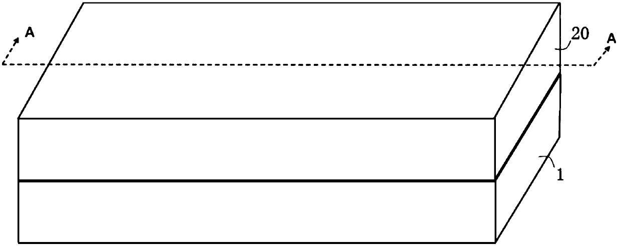
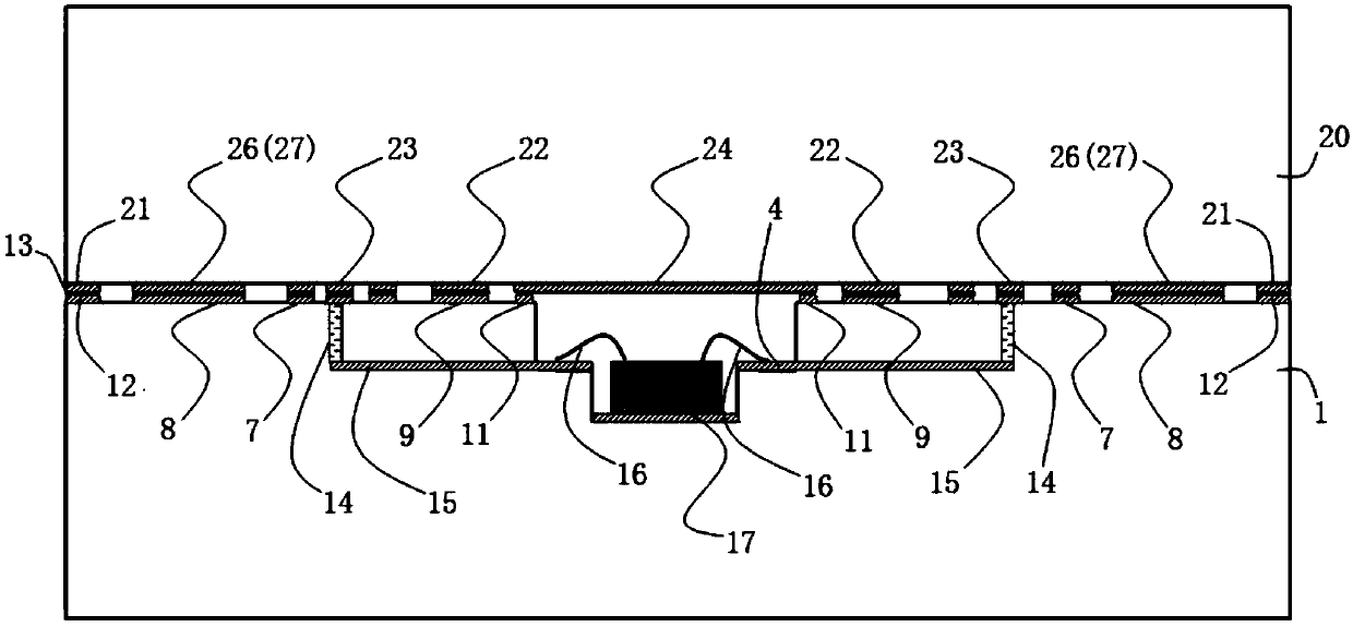
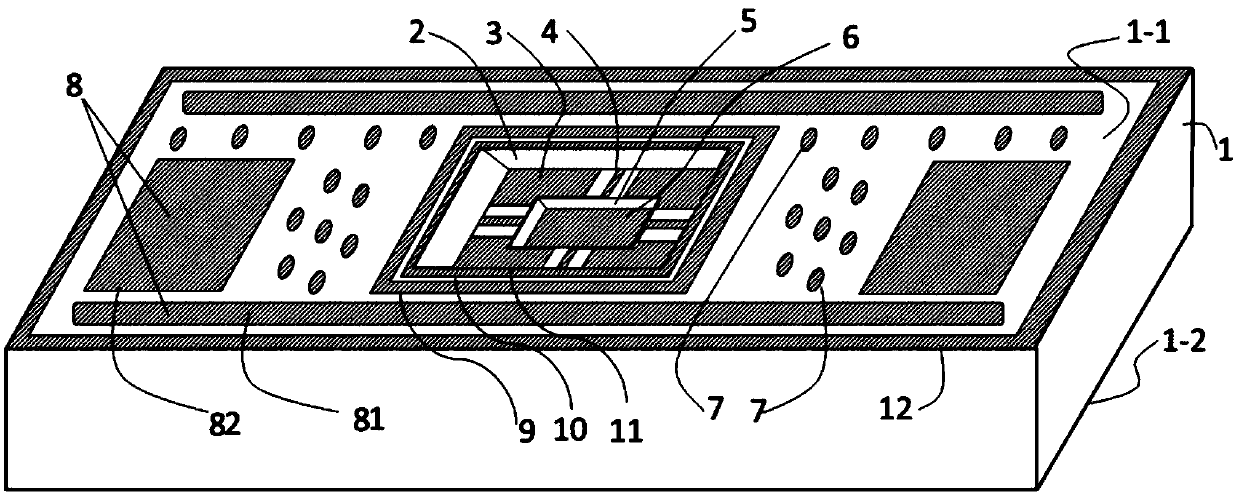
[0047] Such as Figure 1-6 As shown, the three-dimensional stacked structure of LTCC substrates provided by the present invention has scientific and reasonable design, simple structure, and is convenient to use. Integration provides a simple, reliable solution. The three-dimensional stacked structure of LTCC substrates of the present invention includes a first LTCC substrate 1 on which components 17 are placed, and a second LTCC substrate 20 hermetically sealed on the top surface of the first LTCC substrate 1 .

[0048] The top surface of the first LTCC substrate 1 of the present invention is provided with a cavity for placing components 17, the top surface of the cavity is open, and the top surface of the first LTCC substrate 1 is arranged around the opening of ...


PUM

PropertyMeasurementUnit
thicknessaaaaaaaaaa
thicknessaaaaaaaaaa
thicknessaaaaaaaaaa

Abstract

A LTCC substrate three-dimensional stacking structure and a hermetic packaging method thereof are disclosed. The three-dimensional stacking structure comprises components, first and second LTCC substrates, first, second, third, fourth, fifth and sixth metal film layer, and first and second pads. The hermetic packaging method comprises the following steps of: processing a substrate with a ceramic dummy layer on a stacked assembly surface by a conventional LTCC proces; grinding and leveling the surface of the assembly surface; fabricating metallized pads for solder welding on the assembly surface by a post-firing process; prefusing the solder in the welding area and performing cleaning; assembling the components on the substrate; aligning the stacking assembling surfaces of the substrates with assembled components and performing heating to realize sol bonding; cleaning the weld seam and supplementing the solder; testing the airtightness of the stacked LTCC substrates, and welding the substrates until the substrates are qualified if the airtightness is not up to the standard. The invention can realize the vertical interconnection between the local hermetic package of the substrate and the substrate including the high-frequency signal, and provides a simple and reliable solution for the high-density integration.

Description

technical field [0001] The invention relates to the field of LTCC substrate processing and assembly, in particular to a three-dimensional stacked structure of an LTCC substrate and a hermetic packaging method thereof. Background technique [0002] LTCC technology has been widely used in miniaturized microwave fields such as aviation, spaceflight, and missile-borne due to its excellent high-frequency performance, high integration density, and high reliability. With the continuous development of multi-functional and high-density integration trends, the traditional hybrid integration method can no longer meet the needs of products, especially in order to realize the hermetic packaging of bare chips, it is often necessary to seal the LTCC substrate as a whole to the metal box Among them, the interconnection between substrates is realized by a large number of connectors and cables, which not only greatly weakens the miniaturization of the product, but also increases the difficult...

Claims


Application Information

Patent Timeline
Patent Type & Authority Applications(China)
IPC IPC(8): H01L23/488H01L23/522H01L21/56
CPCH01L21/56H01L23/488H01L23/522H01L2224/48091H01L2224/73265H01L2924/00014
Inventor 岳帅旗王娜杨宇刘志辉张英华
Owner SOUTHWEST CHINA RES INST OF ELECTRONICS EQUIP
Why Eureka
Try Eureka