A method for reduce spherical defects in deep submicron photolithography process
A photolithography process and spherical defect technology, applied in photosensitive material processing, pattern surface photoengraving process, photoengraving process coating equipment, etc. , to ensure consistency, to ensure the effect of production capacity
- Summary
- Abstract
- Description
- Claims
- Application Information
AI Technical Summary
Problems solved by technology
Method used
Image
Examples
Embodiment 1
[0067] 1) Place the wafer on the 23°C cold plate in the gluing chamber of the gluing and developing all-in-one machine for cooling pretreatment before gluing, and the time is 60s;
[0068] 2) Coat the bottom anti-reflection coating on the wafer in the coating chamber and let it stand for 50s;
[0069] 3) Baking the finished wafer on a 180°C high-temperature hot plate for 60s to evaporate the solvent in the anti-reflective coating;
[0070] 4) Transfer the wafer to the cold plate to lower the temperature to room temperature to prepare for the next process;
[0071] 5) The required photoresist coating is carried out on the wafer, so that the graphics on the photoresist plate are printed into the film after exposure;
[0072] 6) Transfer the wafer to a 90°C low-temperature hot plate and bake for 60s to discharge the water vapor and other liquids in the adhesive layer;
[0073] 7) Transfer the wafer to a 23°C cold plate to cool to room temperature;
[0074] 8) Expose the photor...
Embodiment 2
[0082] Present embodiment is identical with embodiment 1 except step 2), and step 2) is in the present embodiment:
[0083] Coat the bottom anti-reflection coating on the wafer in the coating chamber and let it stand for 60s.
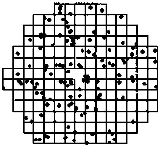
[0084] The spherical defect analysis is carried out on the wafer completed by photolithography in this embodiment, and the spherical defect distribution results can be found in Figure 7 , Through the inspection of defects one by one, the number of spherical defects is significantly reduced compared with the original method, and the number of defects is about 2 to 3, which is acceptable for general semiconductor wafer manufacturing processes.
Embodiment 3
[0086] Present embodiment is identical with embodiment 1 except step 2), and step 2) is in the present embodiment:
[0087] Coat the bottom anti-reflection coating on the wafer in the coating chamber and let it stand for 70s.
[0088] The spherical defect analysis is carried out on the wafer completed by photolithography in this embodiment, and the spherical defect distribution results can be found in Figure 8 , Through checking the defects one by one, no spherical defects were found.
[0089] The experiment was repeated 10 times, and the completed wafer was scanned for defects and reviewed for defects, and no spherical defects were found. in, Figure 9 It is a schematic diagram of the defect distribution of two of them extracted, Figure 9 (a) Schematic diagram of the distribution of spherical defects in the first experiment, Figure 9 (b) is a schematic diagram of the distribution of spherical defects in the eighth experiment.
PUM
 Abstract
Description
Claims
Application Information
 - R&D
- Intellectual Property
- Life Sciences
- Materials
- Tech Scout
- Unparalleled Data Quality
- Higher Quality Content
- 60% Fewer Hallucinations
Browse by: Latest US Patents, China's latest patents, Technical Efficacy Thesaurus, Application Domain, Technology Topic, Popular Technical Reports.
© 2025 PatSnap. All rights reserved.Legal|Privacy policy|Modern Slavery Act Transparency Statement|Sitemap|About US| Contact US: help@patsnap.com


