Cleaning system and cleaning method

A cleaning system and cleaning cylinder technology, which is applied in the fields of electrical components, semiconductor/solid-state device manufacturing, circuits, etc., can solve the problems that semiconductor wafers have not yet formed automatic operations, unfavorable semiconductor wafer processing and production, and different cleaning methods

Pending Publication Date: 2019-01-04
广东长信精密设备有限公司
View PDF0 Cites 2 Cited by
  • Summary
  • Abstract
  • Description
  • Claims
  • Application Information

AI Technical Summary

Problems solved by technology

At present, almost all semiconductor wafers are cleaned manually. Since wafer cleaning has high process requirements, such as: cleaning method, concentration of chemical solution, temperature of chemical solution, cleaning time of chemical solution, flushing time, etc., if artificial Cleaning, everyone has different habits and different cleaning methods, which may affect t

Method used


Image

  • Cleaning system and cleaning method
  • Cleaning system and cleaning method
  • Cleaning system and cleaning method

Examples


Embodiment Construction

[0029] The technical solution will be clearly and completely described below in conjunction with the embodiments of the present invention. Apparently, the described embodiments are only some of the embodiments of the present invention, not all of them. Based on the embodiments of the present invention, all other embodiments obtained by persons of ordinary skill in the art without making creative efforts belong to the protection scope of the present invention.

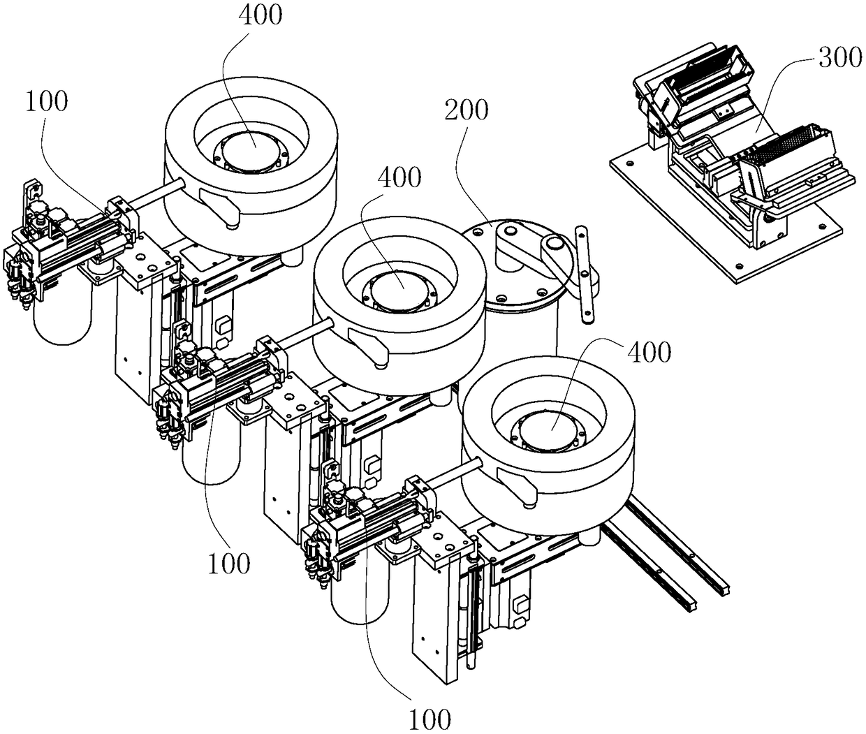
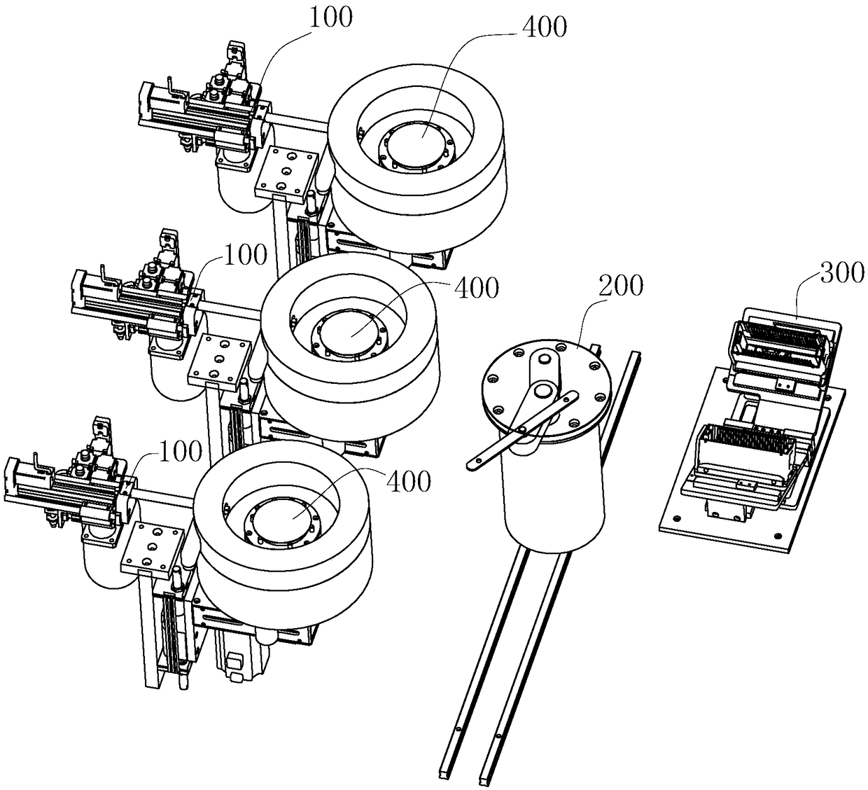
[0030] The present invention proposes a cleaning system for cleaning semiconductor wafers, please refer to Figure 1-2 In this embodiment, the cleaning system is a combination of three cleaning devices 100 , one robotic arm 200 , and one wafer storage device 300 .

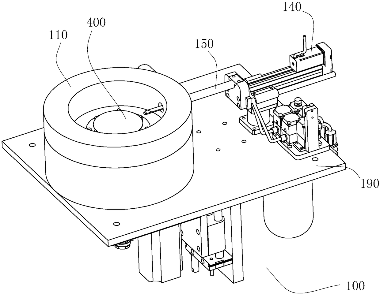
[0031] see Figure 3-4 , the cleaning device 100 is used to clean the wafer 400. The cleaning device 100 includes a cleaning cylinder 110, a liftable and rotatable column 120, a base 130 installed on the column 120, a cylinder 140, and one end is fixed on t...


PUM


Abstract

The invention relates to a cleaning system, which includes at least one cleaning device, at least one robot arm, and at least one wafer access device. The invention also relates to a cleaning method.The cleaning system is composed of the cleaning device, robot arm and wafer access device, realizes automatic transfer and cleaning of the wafers to replace manual cleaning, so as to avoid defects such as water stains, watermarks, pen suction marks and the like on t the wafers after surface cleaning, improve productivity, and reduce production cost.

Description

technical field [0001] The invention relates to the field of semiconductor wafer cleaning, in particular to a semiconductor wafer cleaning system and cleaning method. Background technique [0002] Group III-V compound semiconductor materials represented by gallium arsenide (GaAs) are widely used in the fields of satellite communications, microwave devices, lasers and light-emitting diodes due to their unique electrical properties. The manufacture of devices such as heterojunction bipolar transistors, high electron mobility transistors, and LEDs requires the growth of epitaxial structures on the surface of high-quality substrates by molecular beam epitaxy or organometallic compound vapor phase epitaxy. With the continuous improvement of semiconductor device manufacturing process, the size of the device is getting smaller and higher, and the utilization rate is getting higher and higher. The quality of the semiconductor substrate, especially the quality of the wafer surface, h...

Claims


Application Information

Patent Timeline
IPC IPC(8): H01L21/67
CPCH01L21/67051
Inventor 刘留廖彬周铁军沈艳东
Owner 广东长信精密设备有限公司
Why Eureka
Try Eureka