SiC@SiO2@ferrite high-temperature wave-absorbing composite material and preparation method thereof
A composite material and ferrite technology, applied in chemical instruments and methods, other chemical processes, etc., can solve the problems of no shielding effect, narrow absorbing range, complex preparation process, etc., and achieve controllable absorbing intensity, absorbing The effect of controllable frequency band and simple preparation process
- Summary
- Abstract
- Description
- Claims
- Application Information
AI Technical Summary
Problems solved by technology
Method used
Image
Examples
specific Embodiment approach 1
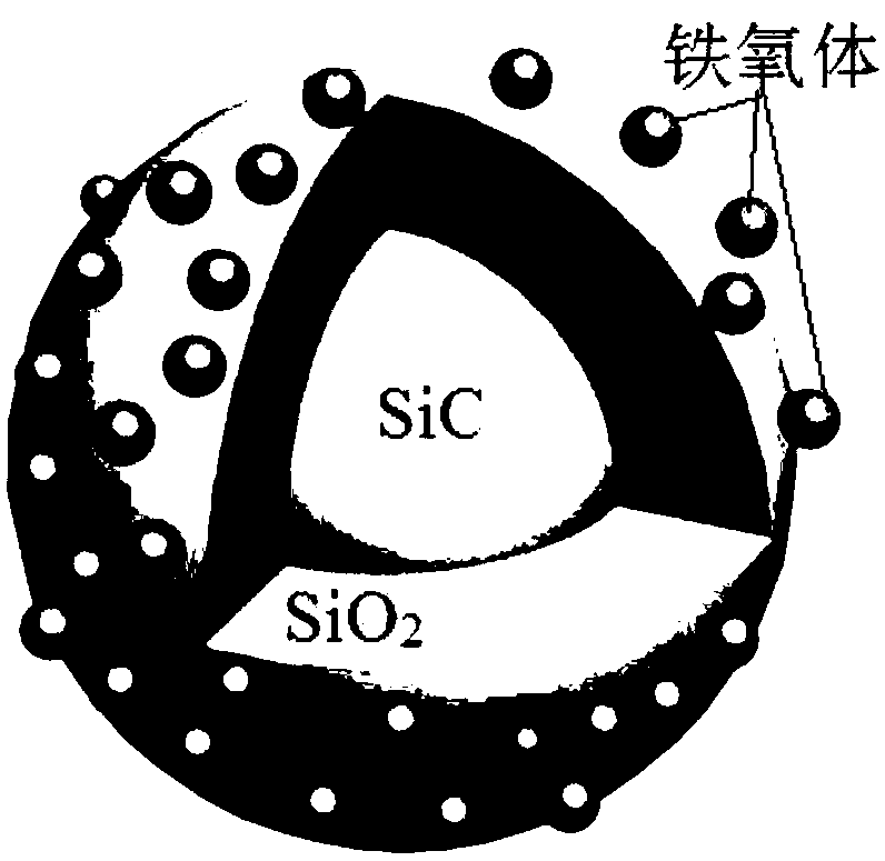
[0040] Specific implementation mode 1: SiC@SiO in this implementation mode 2 @Ferrite high-temperature wave-absorbing composite material, with SiC as the core, and the core is covered with SiO 2 layer, on SiO2 Ferrite particles adhere to the layer.
[0041] SiC@SiO of this embodiment 2 The schematic diagram of the structure of @ferrite high-temperature wave-absorbing composite material is as follows figure 1 shown.
specific Embodiment approach 2
[0042] Embodiment 2: SiC@SiO described in Embodiment 1 2 The preparation method of @ferrite high-temperature wave-absorbing composite material is carried out according to the following steps:
[0043] 1. Silicon carbide surface pretreatment:
[0044] a. Put silicon carbide into a tube furnace, raise the temperature to 200-300°C in air or nitrogen atmosphere and keep it for 2h-4h to oxidize and remove surface impurities;
[0045] b. Disperse silicon carbide in an acidic hydrophilic solution and stir for 2h-4h, then ultrasonically disperse for 1h-2h, then wash with distilled water, filter, and dry to obtain hydrophilic silicon carbide;
[0046] 2. Synthesis of SiC@SiO 2 :
[0047] c. Disperse the hydrophilic silicon carbide into the mixed solvent of alcohol and water, then add the dispersant, cationic surfactant and emulsifier and stir evenly, then add the silane coupling agent, tetraethyl orthosilicate and catalyst, and then mix the solution Continue to stir and react for 6...
specific Embodiment approach 3
[0053] Specific embodiment 3: The difference between this embodiment and specific embodiment 2 is that the silicon carbide in step 1a is α-SiC or β-SiC, wherein α-SiC is 4H type, 15R type or 6H type; other and specific embodiment modes Two same.
PUM
| Property | Measurement | Unit |
|---|---|---|
| Return loss | aaaaa | aaaaa |
Abstract
Description
Claims
Application Information


