Back-illuminated image sensor and forming method thereof

An image sensor and back-illuminated technology, which is applied in the field of image sensors, can solve the problems of complex manufacturing process and improvement, and achieve the effects of simple process, preventing or weakening crosstalk, and easy formation

Inactive Publication Date: 2019-01-11
HUAIAN IMAGING DEVICE MFGR CORP
View PDF8 Cites 5 Cited by
  • Summary
  • Abstract
  • Description
  • Claims
  • Application Information

AI Technical Summary

Problems solved by technology

However, back-illuminated (BSI) image-sensing devices produced by existing methods for manufacturing back-illuminated (BSI) image-sensing devices still have defects. For example, in order to reduce crosstalk between adjacent pixels, several After the pixels, a metal grid will be formed on the back of the semiconductor substrate; and then a color filter will be formed on the metal grid. This manufacturing process is relatively complicated, and the effect of anti-crosstalk needs to be improved.

Method used


Image

  • Back-illuminated image sensor and forming method thereof
  • Back-illuminated image sensor and forming method thereof
  • Back-illuminated image sensor and forming method thereof

Examples


no. 1 example

[0033] Figure 1-7 It is a structural schematic diagram of the formation process of the back-illuminated image sensor according to the first embodiment of the present invention.

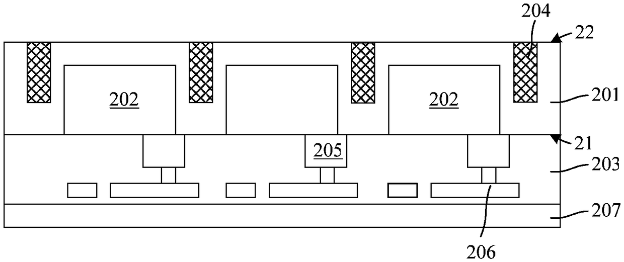
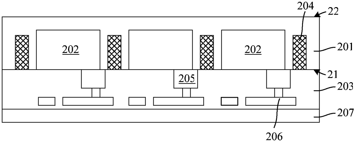
[0034] refer to figure 1, provide a semiconductor substrate 201, the semiconductor substrate 201 includes a first side 21 and a second side 22 opposite to the first side 21, a number of discrete photosensitive regions are formed in the semiconductor substrate 201 of the first side 21 202 , the photosensitive region 202 is suitable for sensing light incident from the second side 22 .

[0035] The material of the semiconductor substrate 201 can be silicon (Si), germanium (Ge), or silicon germanium (GeSi), silicon carbide (SiC); it can also be silicon on insulator (SOI), germanium on insulator (GOI); or It can also be other materials, such as III-V group compounds such as gallium arsenide.

[0036] The semiconductor substrate 201 is doped with impurity ions, and different types of impurity ions are s...

no. 2 example

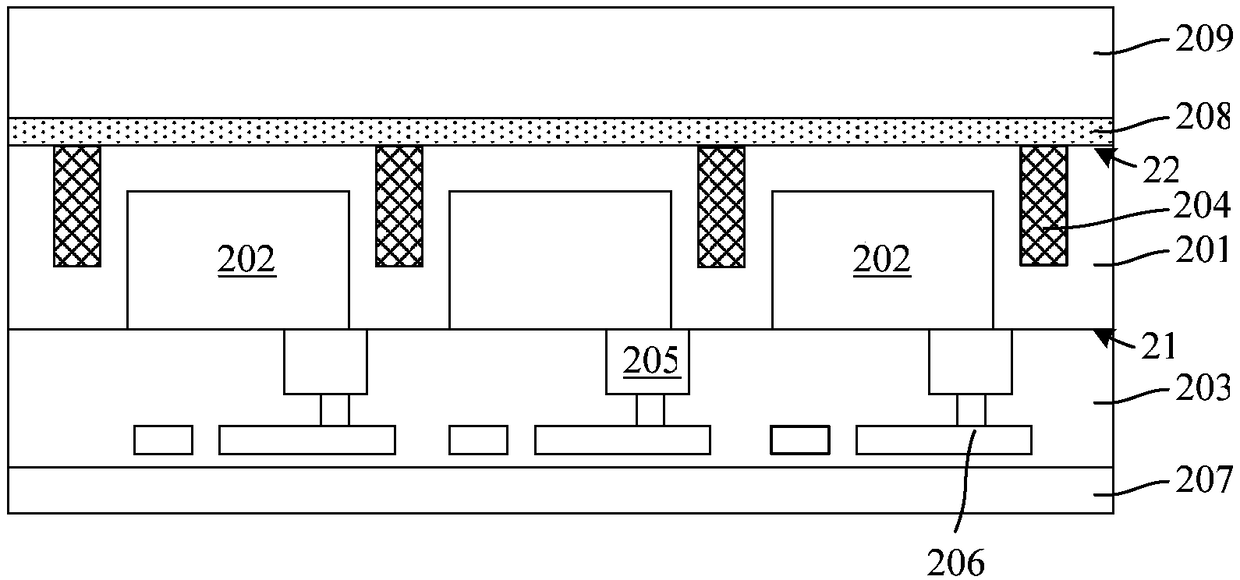
[0062] Figure 8-10It is a schematic structural diagram of the formation process of the back-illuminated image sensor according to the second embodiment of the present invention, Figure 8 is in figure 2 carried out on the basis of The difference between this embodiment and the previous embodiments is that a light-impermeable isolation region 220 is also formed in the first dielectric layer 208 and the semiconductor substrate 201 between the deep trench isolation structure 204 and the light-impermeable spacer 211 , Therefore, the opaque sidewall 211, the opaque isolation region 220 and the deep trench isolation structure 204 form a continuous structure (refer to Figure 10 ), which can further or better prevent the incident light from being transmitted to the adjacent photosensitive area 202, so as to further or better achieve the effect of preventing crosstalk.

[0063] refer to Figure 8 , forming a first dielectric layer 208 on the surface of the second side 22 of the ...


PUM


Abstract

A back-illuminated image sensor and a forming method thereof are provided, the forming method comprising: providing a semiconductor substrate, the semiconductor substrate including a first side and asecond side opposite to the first side, wherein a plurality of discrete photosensitive regions are formed in the semiconductor substrate on the first side, the photosensitive regions being adapted tosense light incident from the second side; Forming a first dielectric layer on a second side surface of the semiconductor substrate; Forming a transparent color filter layer correspondingly on the surface of the first dielectric layer above the partial number of photosensitive regions; Forming a light-absorbing material layer covering surfaces of the transparent color filter layer and the first dielectric layer; Etching the light-absorbing material layer without a mask to form an opaque sidewall on the sidewall surface of the transparent color filter layer; a color filter layer is formed on the surface of the first dielectric layer between the transparent filter layers. The back-illuminated image sensor formed by the method of the invention improves the performance of anti-crosstalk, and has the advantages of simple process and high integration level.

Description

technical field [0001] The invention relates to an image sensor, in particular to a back-illuminated image sensor and a forming method thereof. Background technique [0002] Semiconductor image sensors are used to sense radiation such as light. Complementary metal-oxide semiconductor (CMOS) image sensors (CIS) and charge-coupled device (CCD) sensors are widely used in still digital cameras, camera phones, digital video cameras, medical imaging devices (such as gastroscopes), and automotive imaging devices . These devices utilize an array of pixels (which may include photodiodes (photosensitive regions) and transistors) in the substrate to absorb radiation directed at the substrate and convert the sensed radiation into electrical signals. [0003] A backside illuminated (BSI) image sensing device is one type of image sensing device. Backside illuminated (BSI) image sensing devices can be used to detect light from the backside of the substrate. Compared with front-illumina...

Claims


Application Information

Patent Timeline
Patent Type & Authority Applications(China)
IPC IPC(8): H01L27/146
CPCH01L27/1462H01L27/14621H01L27/1463H01L27/1464H01L27/14683
Inventor 丁琦陈世杰黄晓橹
Owner HUAIAN IMAGING DEVICE MFGR CORP
Why Eureka
Try Eureka