A silicon carbide MOSFET device and a manufacturing method thereof

A silicon carbide and device technology, which is applied in semiconductor/solid-state device manufacturing, semiconductor devices, electrical components, etc., can solve problems such as high production cost, high power loss, and low work efficiency

Active Publication Date: 2019-01-11
UNIV OF ELECTRONICS SCI & TECH OF CHINA
View PDF11 Cites 11 Cited by
  • Summary
  • Abstract
  • Description
  • Claims
  • Application Information

AI Technical Summary

Problems solved by technology

[0007] The present invention needs to be solved, that is, aiming at the above problems, on the basis of the silicon carbide UMOSFET structure, a method that can optimize the

Method used


Image

  • A silicon carbide MOSFET device and a manufacturing method thereof
  • A silicon carbide MOSFET device and a manufacturing method thereof
  • A silicon carbide MOSFET device and a manufacturing method thereof

Examples


Embodiment 1

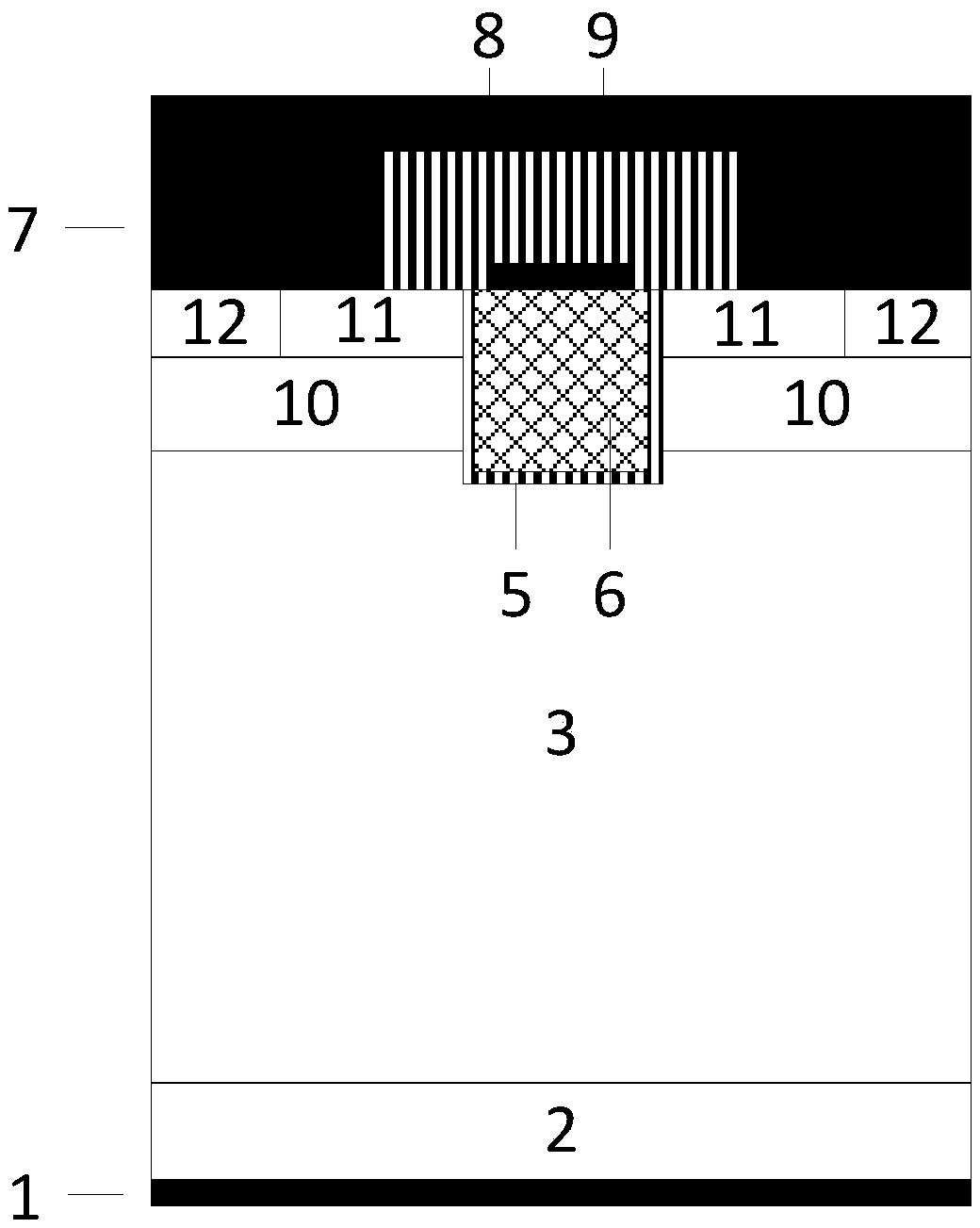
[0071] Such as figure 2 As shown, a silicon carbide MOSFET device, the cell structure includes drain metal 1, silicon carbide N + Substrate 2 and SiC N - epitaxial layer 3; the silicon carbide N - There is a silicon carbide P+ region 4 on the upper left of the epitaxial layer 3, and the silicon carbide N - The upper right of the epitaxial layer 3 has a mesa structure, the mesa structure includes a silicon carbide Pbase region 10, a silicon carbide N+ source region 11 and a silicon carbide P+ contact region 12, and the silicon carbide N+ source region 11 and silicon carbide P+ contact region 12 are located Above the silicon carbide Pbase region 10, on the left side of the mesa structure, silicon carbide N - There is a gate structure above the epitaxial layer 3, and the gate structure includes a gate dielectric layer 5, a polysilicon gate 6, and a gate electrode 9. The polysilicon gate 6 is surrounded by the gate dielectric layer 5, and its upper part is drawn out through th...

Embodiment 2

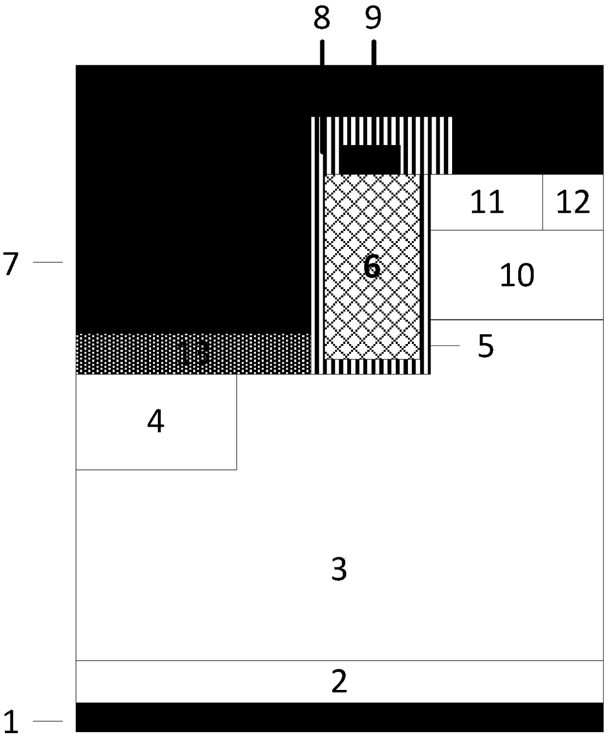
[0073] The structure of this embodiment is substantially the same as that of Embodiment 1, except that the Schottky contact metal 13 has a larger lateral dimension, and the right side of the Schottky contact metal 13 covers the bottom region of the gate structure. Such as image 3 shown. This setting increases the Schottky contact area while reducing the cell area, so that the device has better on-state characteristics.

Embodiment 3

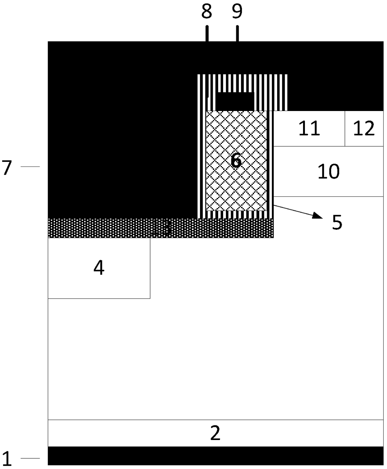
[0075] The structure of this embodiment is substantially the same as that of Embodiment 1, except that the bottom region of the gate structure has a silicon carbide P+ region 4, such as Figure 4 shown. This improvement is beneficial to the further protection of the gate structure and the Schottky contact metal 13, so as to improve the long-term reliability of the device;


PUM

PropertyMeasurementUnit
Thicknessaaaaaaaaaa
Widthaaaaaaaaaa
Thicknessaaaaaaaaaa

Abstract

The invention provides a silicon carbide MOSFET device and a manufacturing method thereof. The invention improves device structure design and finally integrates Schottky contact or heterojunction contact with rectifying characteristics on the basis of traditional silicon carbide UMOSFET structure. At that same time of optimize the basic characteristics of the traditional silicon carbide UMOSFET structure, the improvement realize the integration of multi-sub rectifier devices, greatly optimizes the work performance of the third quadrant of the device, and in addition, the invention also optimizes the dynamic performance of the device, and has shorter switching time; In addition, the invention also has the characteristics of simple process and easy realization.

Description

technical field [0001] The invention belongs to power semiconductor technology, in particular, relates to a metal oxide semiconductor field effect (MOSFET) device structure and a manufacturing method thereof. Background technique [0002] The anthropocene has entered the 21st century. Although various forms of new energy sources have emerged, such as wind energy, nuclear energy, solar energy, and geothermal energy, the world's energy production and consumption are still dominated by fossil energy, and fossil energy will remain in the long run. For a period of time, it occupies the most important seat of many energy needs of human beings. The large and long-term use of fossil energy will inevitably lead to a series of problems, which are closely related to the deterioration of global environmental problems such as global warming. A considerable proportion of fossil energy is converted into electricity. Electric energy is one of the main forms of energy that can be directly ...

Claims


Application Information

Patent Timeline
IPC IPC(8): H01L29/78H01L29/24H01L29/06H01L21/265H01L21/336
CPCH01L21/26513H01L29/0688H01L29/24H01L29/66704H01L29/7806H01L29/7813
Inventor 张金平邹华罗君轶赵阳李泽宏张波
Owner UNIV OF ELECTRONICS SCI & TECH OF CHINA
Why Eureka
Try Eureka