Screening and packaging device for production of chip thermo-sensitive resistors

A thermistor and screening device technology, which is applied in packaging, magnetic separation, solid separation, etc., can solve the problems of easy falling, inaccurate screening, and good products that cannot be further classified, and achieve the effect of reducing damage

Inactive Publication Date: 2019-01-18
溧阳市超强链条制造有限公司
View PDF0 Cites 3 Cited by
  • Summary
  • Abstract
  • Description
  • Claims
  • Application Information

AI Technical Summary

Problems solved by technology

[0004] In order to solve the above problems, the present invention provides a screening and packaging device for the production of chip thermistors, which can solve the problem that the screening of chip resistors is not accurate enough during magnetic screening, and the screened good products cannot be further classified; The claws will cause damage to the finished product, and the clamping device shakes and falls easily when clamping. It can realize the function of automatic screening and packaging of chip resistors. It has the functions of accurate screening, detailed classification, firm absorption and less damage during packaging. The advantages

Method used


Image

  • Screening and packaging device for production of chip thermo-sensitive resistors
  • Screening and packaging device for production of chip thermo-sensitive resistors
  • Screening and packaging device for production of chip thermo-sensitive resistors

Examples


Embodiment Construction

[0027] In order to make the technical means, creative features, goals and effects achieved by the present invention easy to understand, the present invention will be further described below in conjunction with specific illustrations. It should be noted that, in the case of no conflict, the embodiments in the present application and the features in the embodiments can be combined with each other.

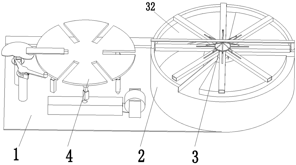
[0028] Such as Figure 1 to Figure 8 As shown, a screening and packaging device for chip thermistor production includes a base plate 1, a detection device 2, a screening device 3 and a packaging device 4, a detection device 2 is installed on the right end of the upper end surface of the base plate 1, and the detection device 2 A screening device 3 is installed on the upper end, and a packaging device 4 is installed on the left end of the upper end surface of the bottom plate 1 .

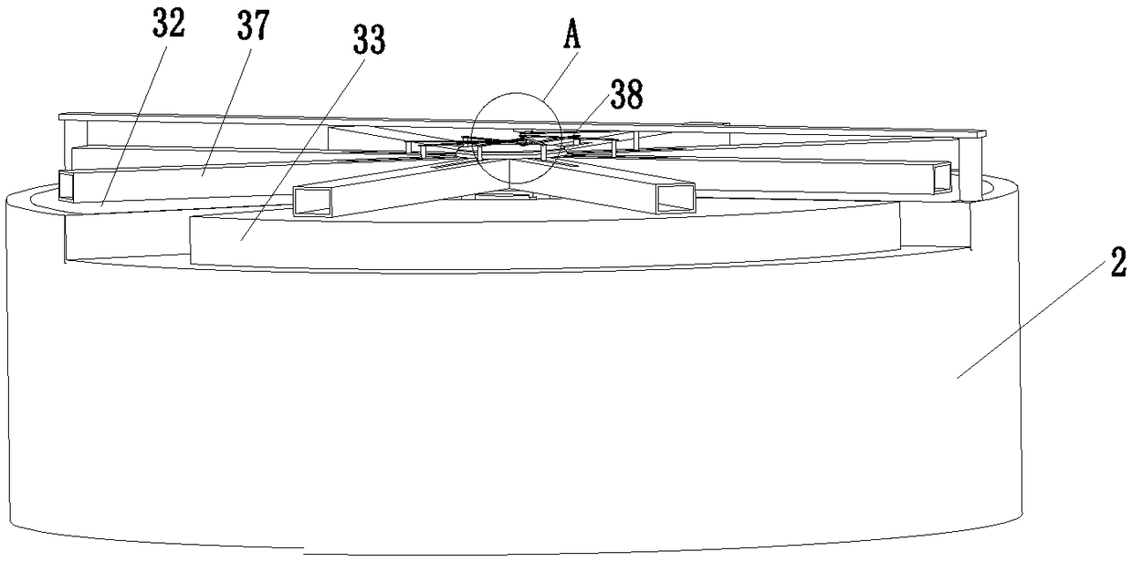
[0029] The screening device 3 includes a support platform 31, the middle part of the detection device 2...


PUM


Abstract

The invention relates to a screening and packaging device for production of chip thermo-sensitive resistors. The screening and packaging device comprises a bottom plate, a detection device, a screening device and a packaging device, wherein the detection device is arranged at the right end of the upper end surface of the bottom plate; the screening device is arranged at the upper end of the detection device; the packaging device is arranged at the left end of the upper end surface of the bottom plate; the screening device comprises a support table; a support table is arranged in the middle part of the detection device; the back end of the upper end surface of the detection device is provided with three material inlets from left to right; a conveying table is arranged at the front end of the upper end surface of the detection device. The screening and packaging device has the advantages that the problems of inaccuracy in magnetic screening of chip resistors, failure in further classifying of screened qualified products, damage to the finished products by clamping jaws in packaging, easiness in falling due to shaking of a clamping device in clamping and the like are solved; the automatic screening and packaging function is realized for the chip resistors; the screening is precise, and the classifying is detailed; during packaging, the suction is firm, the easiness in falling is avoided, and the damage is reduced.

Description

technical field [0001] The invention relates to the field of electronic components, in particular to a screening and packaging device for the production of patch thermistors. Background technique [0002] SMD resistors are scientifically called chip fixed resistors. They have the advantages of moisture resistance, high temperature resistance, high reliability, precision, and small temperature coefficient and resistance tolerance. Layer printing and drying, primary protective layer printing and drying, laser correction, secondary protective layer printing and drying, resistance code printing, vacuum sputtering, magnetic screening, resistance testing and packaging into bags, etc., and the existing production equipment is used throughout the production The magnetic screening in the process and the packaging and bagging process have the following defects. [0003] Existing production equipment uses the magnetism of nickel to screen out defective products, but the screening proc...

Claims


Application Information

Patent Timeline
IPC IPC(8): B03C1/04B65B35/18B65B35/26
CPCB03C1/04B65B35/18B65B35/26
Inventor 毕永光蒋俊美蒋阿生
Owner 溧阳市超强链条制造有限公司
Why Eureka
Try Eureka