

Reflow soldering simulation optimization method, system, computer storage medium and apparatus
An optimization method, reflow soldering technology, applied in computer-aided design, calculation, CAD circuit design, etc., to achieve the effect of improving manufacturing quality and manufacturing efficiency
- Summary
- Abstract
- Description
- Claims
- Application Information
AI Technical Summary
Problems solved by technology
Method used
Image

Examples
Embodiment 1
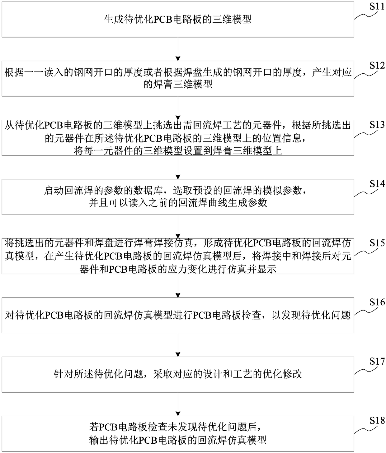
[0038] This embodiment provides a simulation optimization method for reflow soldering, including:
[0039] Generate a 3D model of the PCB circuit board to be optimized;
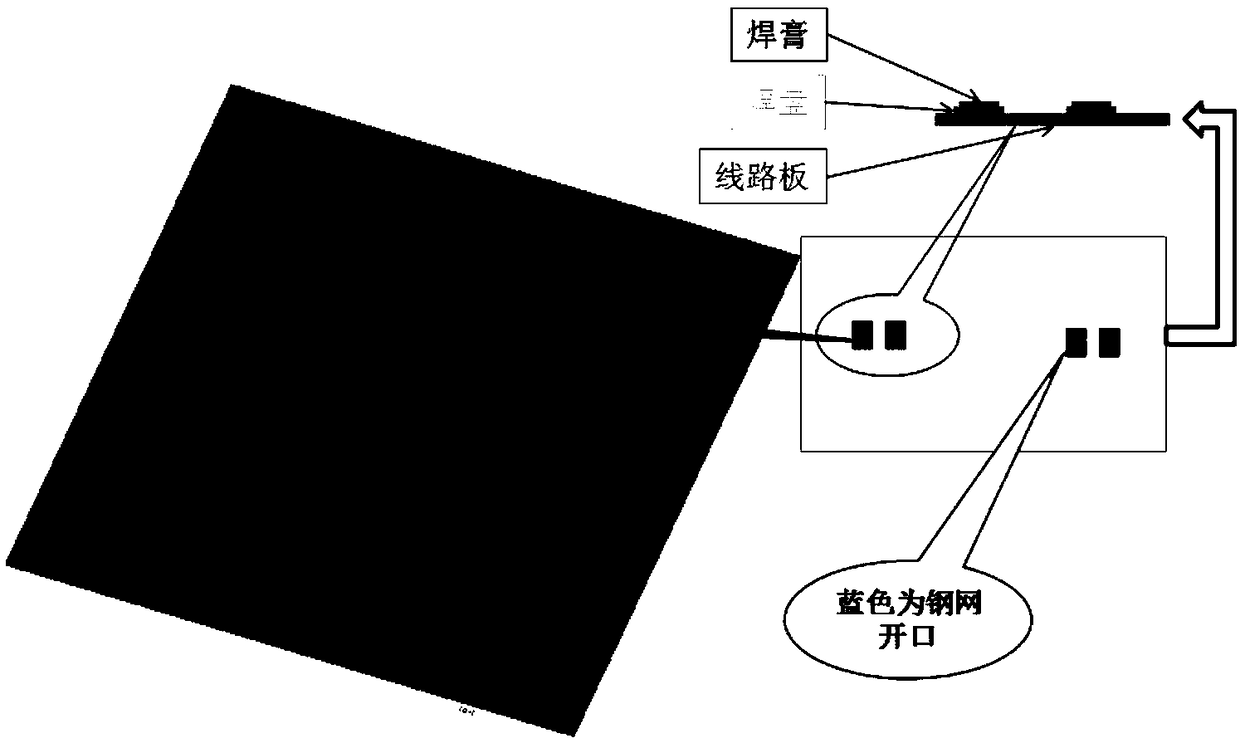
[0040] According to the thickness of the stencil opening read in one by one or the thickness of the stencil opening generated according to the pad, a corresponding three-dimensional model of the solder paste is generated;
[0041] From the three-dimensional model of the PCB circuit board to be optimized, select the components that require a reflow soldering process, and place each of the components according to the position information of the selected components on the three-dimensional model of the PCB circuit board to be optimized. Set on the 3D model of solder paste;
[0042]According to the preset simulation parameters of reflow soldering, the selected components and pads are simulated for solder paste soldering to form a reflow soldering simulation model of the PCB circuit board to be optimized;
[004...
Embodiment 2
[0080] This embodiment provides a simulation optimization system for reflow soldering, including:
[0081] Generate module, be used for generating the three-dimensional model of PCB circuit board to be optimized;
[0082] The generation module is used to generate a corresponding three-dimensional model of solder paste according to the thickness of the stencil openings read in one by one or the thickness of the stencil openings generated according to the pad;
[0083] The setting module is used to select components that need a reflow soldering process from the three-dimensional model of the PCB circuit board to be optimized, and according to the position information of the selected components on the three-dimensional model of the PCB circuit board to be optimized, each The components are arranged on the three-dimensional model of the solder paste;
[0084] The simulation module is used to perform solder paste soldering simulation on the selected components and pads according t...
Embodiment 3
[0108] This embodiment provides a device, which includes: a processor, a memory, a transceiver, a communication interface or / and a system bus; the memory and the communication interface are connected to the processor and the transceiver through the system bus and complete mutual communication, and the memory The computer program is stored, the communication interface is used to communicate with other devices, the processor and the transceiver are used to run the computer program, so that the device executes the various steps of the simulation optimization method for reflow soldering described in the first embodiment.
[0109] The system bus mentioned above may be a Peripheral Component Interconnect (PCI for short) bus or an Extended Industry Standard Architecture (EISA for short) bus or the like. The system bus can be divided into address bus, data bus, control bus and so on. The communication interface is used to realize the communication between the database access device an...
PUM
 Abstract
Description
Claims
Application Information