A high-speed transistor and a manufacturing method thereof

A manufacturing method and transistor technology, applied in the field of electronics, can solve problems such as small band gap and poor stability of high-speed transistors, and achieve the effects of increasing breakdown voltage, reducing requirements, and improving frequency and power performance

Pending Publication Date: 2019-01-18
深圳市华讯方舟智能信息技术有限公司
View PDF0 Cites 2 Cited by
  • Summary
  • Abstract
  • Description
  • Claims
  • Application Information

AI Technical Summary

Problems solved by technology

[0004] The invention provides a high-speed transistor and its manufacturing method, aiming to solve the problem of poor stability of the high-speed transistor caused by the small band gap of indium tin oxide and zinc oxide in the traditional high-speed transistor

Method used


Image

  • A high-speed transistor and a manufacturing method thereof
  • A high-speed transistor and a manufacturing method thereof
  • A high-speed transistor and a manufacturing method thereof

Examples


Embodiment Construction

[0045] In order to make the object, technical solution and advantages of the present invention clearer, the implementation manner of the present invention will be further described in detail below in conjunction with the accompanying drawings.

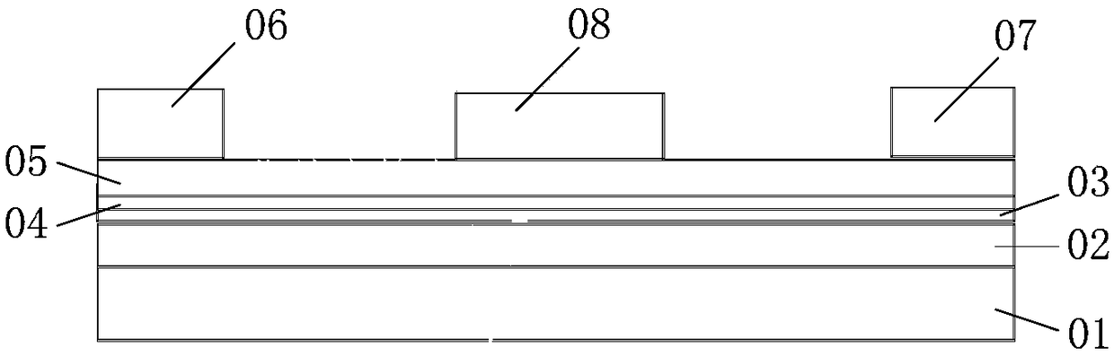
[0046] figure 1 The module structure of the high-speed transistor provided by the embodiment of the present invention is shown. For the convenience of description, only the parts related to the embodiment of the present invention are shown. The details are as follows:

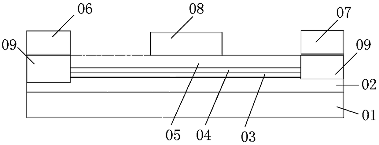
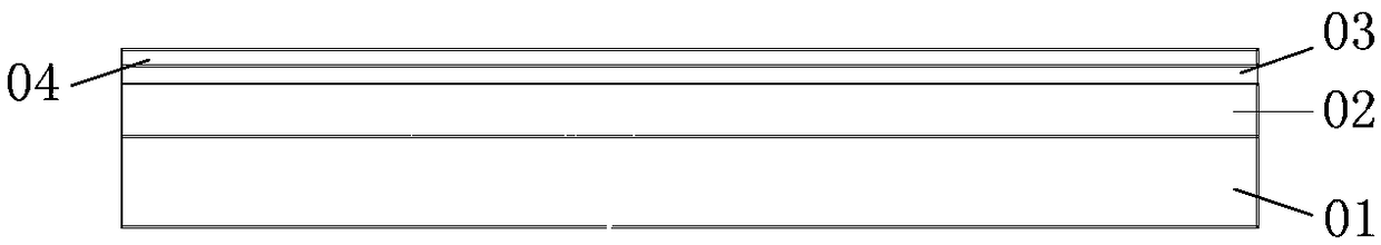
[0047] The high-speed transistor includes a substrate layer 01, a channel layer 02, a first non-doped (Al x Ga 1-x ) 2 o 3 Layer 03, highly doped (Al x Ga 1-x ) 2 o 3layer 04 , voltage modulation layer 05 , source electrode 06 , drain electrode 07 and gate electrode 08 .

[0048] Wherein, the channel layer 02 is arranged on the upper surface of the substrate layer 01; the first non-doped (Al x Ga 1-x ) 2 o 3 Layer 03 is arranged on the upper surface of chann...


PUM


Abstract

The invention belongs to the field of electronic technology and discloses a high-speed transistor and a manufacturing method thereof. The high-speed transistor comprises a substrate laye; a channel layer disposed on the upper surface of the substrate layer; a first undoped (AlxGa1-x) 2O3 layer disposed on the upper surface of the channel layer; a highly doped (AlxGa1-x) 2O3 layer disposed on the upper surface of the first undoped (AlxGa1-x) 2O3 layer; a voltage modulation layer disposed on the upper surface of the highly doped (AlxGa1-x) 2O3 layer; a source electrode and a drain electrode spaced apart on an upper surface of the voltage modulation layer; and a gate electrode disposed on the upper surface of the voltage modulation layer and located in a region between the source electrode and the drain electrode; As that novel high-speed and high-power transistor are fabricated by the ultra-wide band-gap semiconductor material system and the high-doping (AlxGa1-x) 2-D heterojunction electron gas is formed by the modulation of 2O 3 layer, which effectively improves the frequency and power performance of the device, improves the breakdown voltage of the device material, reduces the requirement of device packaging, and increases the market competitiveness of the device.

Description

technical field [0001] The invention belongs to the field of electronic technology, and in particular relates to a high-speed transistor and a manufacturing method thereof. Background technique [0002] A high-speed transistor on the conventional market has a driving unit having an active layer formed in a structure in which a first oxide semiconductor layer and a second oxide semiconductor layer are stacked, wherein the first oxide semiconductor layer is selected from indium tin oxide , the second oxide semiconductor layer is selected from zinc oxide. Due to the small bandgap width of indium tin oxide and zinc oxide, the breakdown voltage of the device material itself is small, and the frequency performance and power performance are poor, resulting in poor stability of high-speed transistors. [0003] Traditional high-speed transistors have the defect that the bandgap of indium tin oxide and zinc oxide is small, which leads to poor stability of high-speed transistors. Co...

Claims


Application Information

Patent Timeline
Patent Type & Authority Applications(China)
IPC IPC(8): H01L29/778H01L29/24H01L21/34
CPCH01L29/7786H01L29/24H01L29/66969
Inventor 张宇丁庆吴光胜冯军正蓝永海
Owner 深圳市华讯方舟智能信息技术有限公司
Why Eureka
Try Eureka