Flash memory system and method for image convolution operation assisted by adder

A technology of convolution operation and adder, which is applied in the field of semiconductor integrated circuits and its manufacturing, can solve problems such as threshold voltage drop, threshold voltage rise, and convolution calculation accuracy cannot be guaranteed, so as to reduce the impact of calculation accuracy and increase The effect of robustness

Active Publication Date: 2020-09-11
PEKING UNIV
View PDF11 Cites 0 Cited by
  • Summary
  • Abstract
  • Description
  • Claims
  • Application Information

AI Technical Summary

Problems solved by technology

People have proposed a coded flash memory system based on the analog operation of the NOR Flash structure, but in this implementation, when the NOR Flash unit performs PROGRAM programming operations, it will be in the floating gate layer during the tunneling process. The introduction of movable charges will cause the threshold voltage to rise, and when the ERASE erase operation is performed, the movable charges introduced during the tunneling process will be erased, and the threshold voltage will drop
Therefore, when the threshold fluctuation between NOR Flash units is high, the accuracy of convolution calculation becomes unguaranteed, which increases the complexity of output unit design

Method used


Image

  • Flash memory system and method for image convolution operation assisted by adder
  • Flash memory system and method for image convolution operation assisted by adder
  • Flash memory system and method for image convolution operation assisted by adder

Examples


specific Embodiment

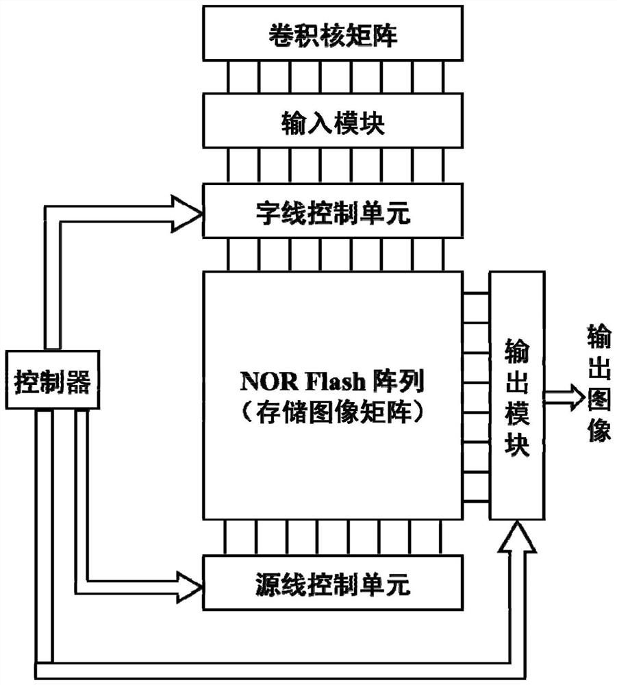
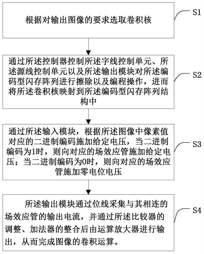
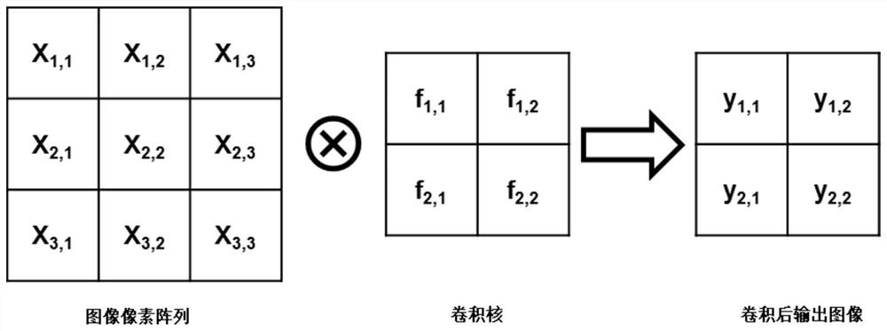
[0031] Such as image 3 Shown is a schematic diagram of the principle of pixel matrix convolution according to an embodiment of the present invention. Wherein, a 3×3 size image pixel array is processed by a 2×2 size convolution kernel to obtain a 2×2 size output image pixel matrix. In the NOR Flash array circuit structure, each pixel in the 3×3 image pixel array is converted into a corresponding electrical signal and then input by a word line, so 9 word lines are required. In the process of convolution operation, the convolution kernel must be rotated 180 degrees first, and then multiplied by the pixels in the corresponding position in the 2×2 size of the input image matrix, and then accumulated. The product kernel is multiplied with the corresponding position of the 2×2 part of the image matrix in order from left to right and from top to bottom, and then accumulated, and finally an output image pixel matrix with a size of 2×2 is obtained. , the process can be expressed as: ...


PUM


Abstract

An adder-aided flash memory system and method for implementing image convolution operation are disclosed, wherein the system comprises an input module, an encoded flash memory array, a controller, a word line control unit, a source line control unit and an output module, wherein the encoded flash memory array is composed of no less than 2 SKm2 (m n+1) field effect transistors arranged in the array. The output module comprises no less than 2K (m n+1) adder, corresponding number of comparators and operational amplifiers, and the encoded flash memory array is connected with the comparator throughbit lines, thereby being connected with the output module. The method comprises: applying a given voltage according to a binary code corresponding to pixel values in the image through the input module, and making only one corresponding field effect transistor on the same bit line at the same time operate through the control of a controller. In this way, the influence of NOR Flash element fluctuation on computational accuracy is effectively reduced, and the robustness of convolution computation system is improved.

Description

technical field [0001] The invention belongs to the technical field of semiconductor integrated circuits and its manufacture, and more specifically relates to a flash memory system and method for implementing image convolution operation assisted by an adder, which are used to realize fast and accurate image convolution. Background technique [0002] Convolution operation is an important operation in analytical mathematics and is widely used in digital signal processing and machine learning. Convolution operation is actually a weighted summation process. In the traditional CPU computing structure, convolution operation is often divided into multiplication and addition operations step by step, so the efficiency of convolution operation is not high. In order to improve the efficiency of convolution operation implementation, a vertical cross array structure is proposed. This structure not only has the advantages of simple fabrication, low cost, high integration density, and eas...

Claims


Application Information

Patent Timeline
Patent Type & Authority Patents(China)
IPC IPC(8): G06F17/15G06T1/60
CPCG06F17/15G06T1/60G06T2200/28
Inventor 黄鹏韩润泽项亚臣康晋锋刘晓彦舒清明胡洪苏志强刘璐
Owner PEKING UNIV
Why Eureka
Try Eureka