LED epitaxial growth method for improvement of growth quality

A technology of epitaxial growth and quality, which is applied in the direction of electrical components, semiconductor/solid-state device manufacturing, circuits, etc. It can solve the problems of high chip grinding fragmentation rate, large warping of epitaxial wafers, and low product yield, so as to improve antistatic ability , improve crystal quality, improve the effect of lattice matching

Inactive Publication Date: 2019-02-01
XIANGNENG HUALEI OPTOELECTRONICS
View PDF4 Cites 3 Cited by
  • Summary
  • Abstract
  • Description
  • Claims
  • Application Information

AI Technical Summary

Problems solved by technology

However, since the low-temperature buffer layer is still hetero-epitaxy, its improved crystal quality is limited.
In addition, due to the large lattice mismatch between the epitaxial film layers, the epitaxial crystal film has been subjected to stress during the growth process, resulting in bending and warping of the epitaxial film.
When the traditional low-temperature buffer layer method is used to grow epitaxial crystals on large-size sapphire substrates, the warpage of the epitaxial wafers is large, resulting in a high rate of grinding fragments and low product yields in the subsequent chip manufacturing process

Method used


Image

  • LED epitaxial growth method for improvement of growth quality
  • LED epitaxial growth method for improvement of growth quality
  • LED epitaxial growth method for improvement of growth quality

Examples


specific Embodiment

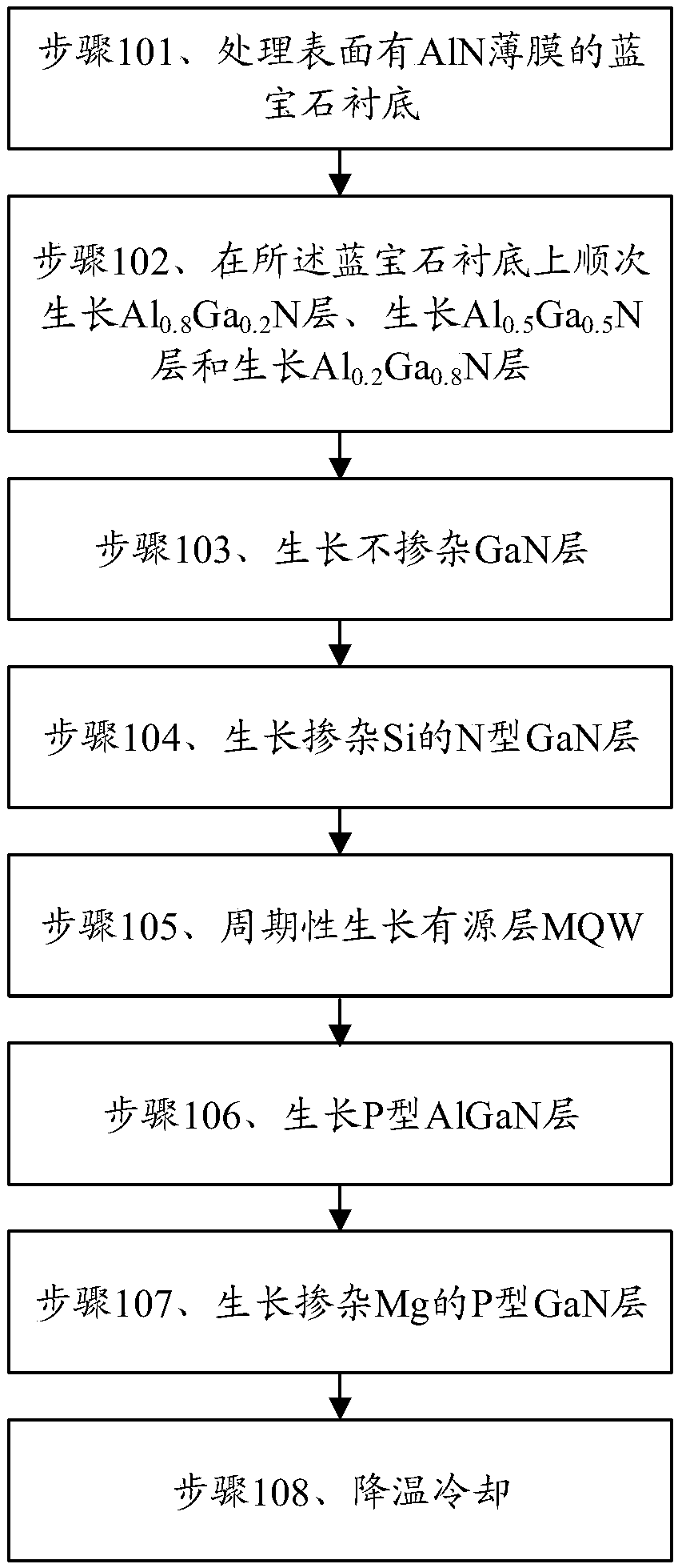
[0040] see figure 1 Shown is a specific embodiment of the LED epitaxial growth method for improving the growth quality described in this application, the method comprising:

[0041] Step 101, processing the sapphire substrate with the AlN thin film on the surface, specifically, treating the sapphire substrate with the AlN thin film on the surface at 1000° C. for 5 minutes under a hydrogen atmosphere with the reaction chamber pressure maintained at 100 mbar.

[0042] Step 102, sequentially growing Al on the sapphire substrate 0.8 Ga 0.2 N layer, grown Al 0.5 Ga 0.5 N layer and grown Al 0.2 Ga 0.8 N layer:

[0043] The grown Al 0.8 Ga 0.2 The N layer includes: control the reaction chamber pressure of 400mbar, and feed NH with a flow rate Q1 of 60L / min into the reaction chamber 3 , N with a flow rate of 90L / min 2 , TMGa of 100 sccm, TMAl source of 230 sccm, the growth temperature is gradually increased from 800 °C to 900 °C by increasing 0.4 °C per second during the gro...

Embodiment 2

[0059] This embodiment provides an LED epitaxial growth method for improving the growth quality, the method comprising:

[0060] Step 201, processing the sapphire substrate with the AlN thin film on the surface, specifically, treating the sapphire substrate with the AlN thin film on the surface at 1200° C. for 10 minutes under a hydrogen atmosphere with the reaction chamber pressure maintained at 150 mbar.

[0061] Step 202, sequentially growing Al on the sapphire substrate 0.8 Ga 0.2 N layer, grown Al 0.5 Ga 0.5 N layer and grown Al 0.2 Ga 0.8 N layer:

[0062] The grown Al 0.8 Ga0.2 The N layer includes: control the reaction chamber pressure of 600mbar, and feed NH with a flow rate Q1 of 70L / min into the reaction chamber 3 , the N flow rate is 95L / min 2 , TMGa of 110 sccm, TMAl source of 250 sccm, the growth temperature is gradually increased from 800 °C to 900 °C by increasing 0.4 °C per second during the growth process, and Al with a thickness D1 of 10 nm is grown ...

Embodiment 3

[0078] Step 301, processing the sapphire substrate with the AlN thin film on the surface, specifically, treating the sapphire substrate with the AlN thin film on the surface at 1100° C. for 7 minutes under a hydrogen atmosphere with the reaction chamber pressure maintained at 125 mbar.

[0079] Step 302, sequentially growing Al on the sapphire substrate 0.8 Ga 0.2 N layer, grown Al 0.5 Ga 0.5 N layer and grown Al 0.2 Ga 0.8 N layer:

[0080] The grown Al 0.8 Ga 0.2 The N layer includes: control the reaction chamber pressure of 500mbar, and feed NH with a flow rate Q1 of 65L / min into the reaction chamber 3 , N with a flow rate of 92.5L / min 2 , TMGa of 105 sccm, TMAl source of 240 sccm, the growth temperature is gradually increased from 800 °C to 900 °C by increasing 0.4 °C per second during the growth process, and Al with a thickness D1 of 9 nm is grown on the sapphire substrate 0.8 Ga 0.2 N layer;

[0081] Keep the reaction chamber pressure and growth temperature co...


PUM


Abstract

The present invention discloses a LED epitaxial growth method for improvement of growth quality. The method comprises the steps of: processing a sapphire substrate of an AlN film at a surface, growingan Al0.8Ga0.2N layer, an Al0.5Ga0.5N layer and an Al0.2Ga0.8N layer in order on the sapphire substrate, growing an un-doped GaN layer and a Si-doped N-type GaN layer, periodically growing an active layer MQW, growing a P-type AlGaN layer, growing a Mg-doped P-type GaN layer, and performing cooling. The method increases the defect blocking and isolation mechanisms when the epitaxial crystal is grown to improve the lattice matching, reduce the dislocation density, reduce the defect proportion and improve the crystalline quality so as to improve the LED light-emitting efficiency, improve the antistatic capacity and improve the epitaxial wafer surface appearance condition. The LED epitaxial growth method for improvement of growth quality is convenient to eliminate the stress accumulative effect of the sapphire substrate on the GaN film so as to reduce the warping of the epitaxial wafer and improve the product yield.

Description

technical field [0001] The invention relates to the technical field of LED epitaxial wafer growth, in particular to an LED epitaxial growth method for improving growth quality. Background technique [0002] The commonly used GaN growth method is patterning on a sapphire substrate. Sapphire crystal is one of the best substrate materials for the growth of GaN epitaxial layer, the third-generation semiconductor material, and its single crystal preparation process is mature. GaN is used as a base material for blue LEDs. Among them, SiC, the substrate material of the GaN epitaxial layer, has a small lattice mismatch with GaN, only 3.4%, but its thermal expansion coefficient is quite different from that of GaN, which is easy to cause GaN epitaxial layer fracture, and the manufacturing cost is high, which is 10% of that of sapphire. times; the cost of the substrate material Si is low, and the lattice mismatch degree with GaN is large, reaching 17%. It is difficult to grow GaN, an...

Claims


Application Information

Patent Timeline
Patent Type & Authority Applications(China)
IPC IPC(8): H01L21/86H01L33/00H01L33/02H01L33/06H01L33/12H01L33/32
CPCH01L21/86H01L33/007H01L33/0075H01L33/02H01L33/06H01L33/12H01L33/32
Inventor 徐平
Owner XIANGNENG HUALEI OPTOELECTRONICS
Why Eureka
Try Eureka