LDMOS and manufacturing method thereof

A conductivity type and substrate technology, which is applied in semiconductor/solid-state device manufacturing, electrical components, circuits, etc., can solve problems such as low reliability, high electric field strength in the depletion layer, and easy breakdown of devices, so as to reduce the peak electric field , Improving the withstand voltage capacity and reducing the electric field strength

Inactive Publication Date: 2019-02-01
SHENZHEN NANSHUO MINGTAI TECH CO LTD
View PDF5 Cites 6 Cited by
  • Summary
  • Abstract
  • Description
  • Claims
  • Application Information

AI Technical Summary

Problems solved by technology

[0003] In order to increase the breakdown voltage of LDMOS, a drift region is usually added between the source region and the drain region. When a reverse bias is applied between the source and drain, the drift region will form a depletion layer, and the depletion layer has two depletion layers. The distance between two depletion lines determines the e

Method used


Image

  • LDMOS and manufacturing method thereof
  • LDMOS and manufacturing method thereof
  • LDMOS and manufacturing method thereof

Examples


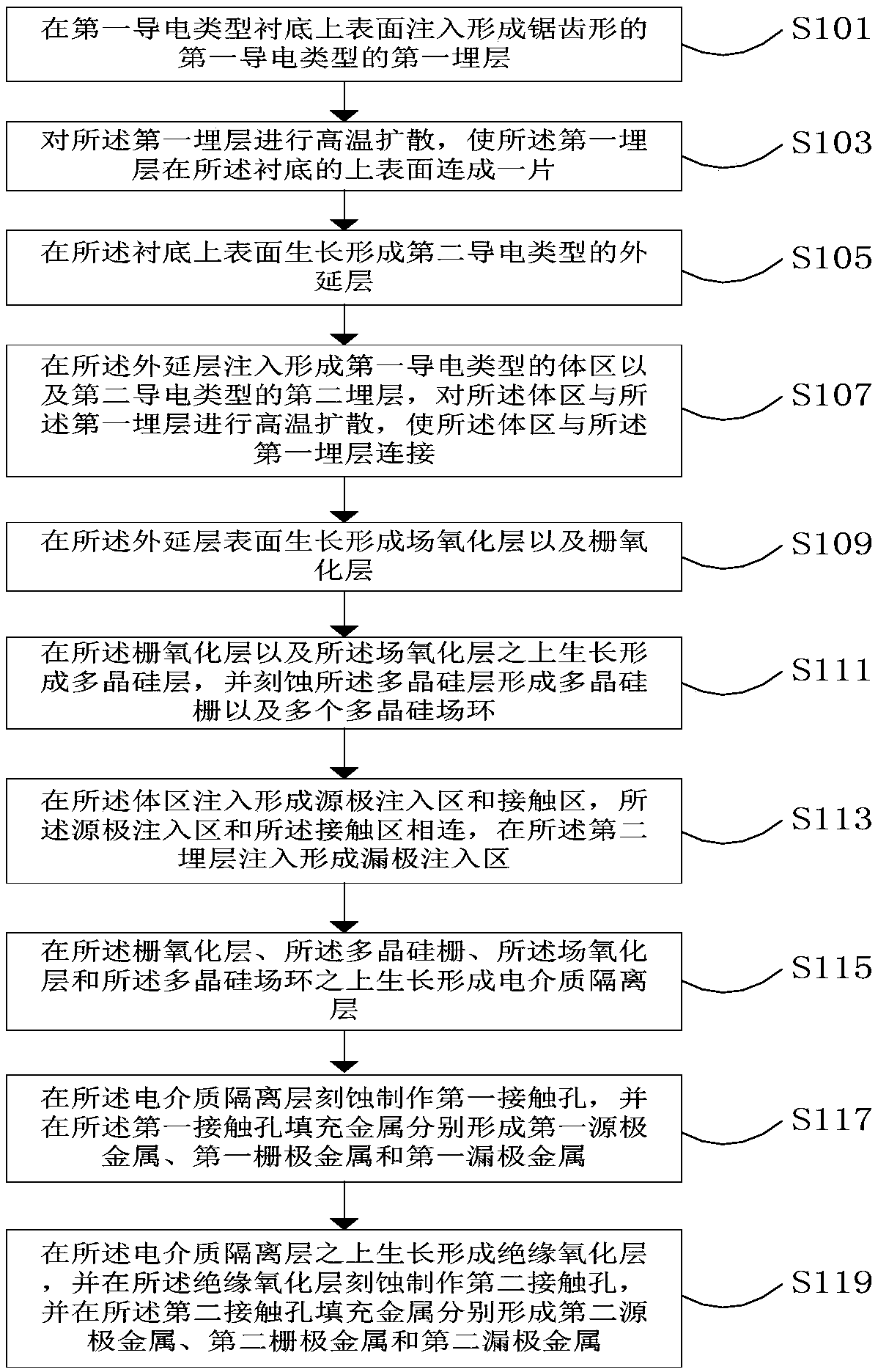
Embodiment Construction

[0051] It should be noted that, in the case of no conflict, the embodiments of the present invention and the features in the embodiments can be combined with each other.

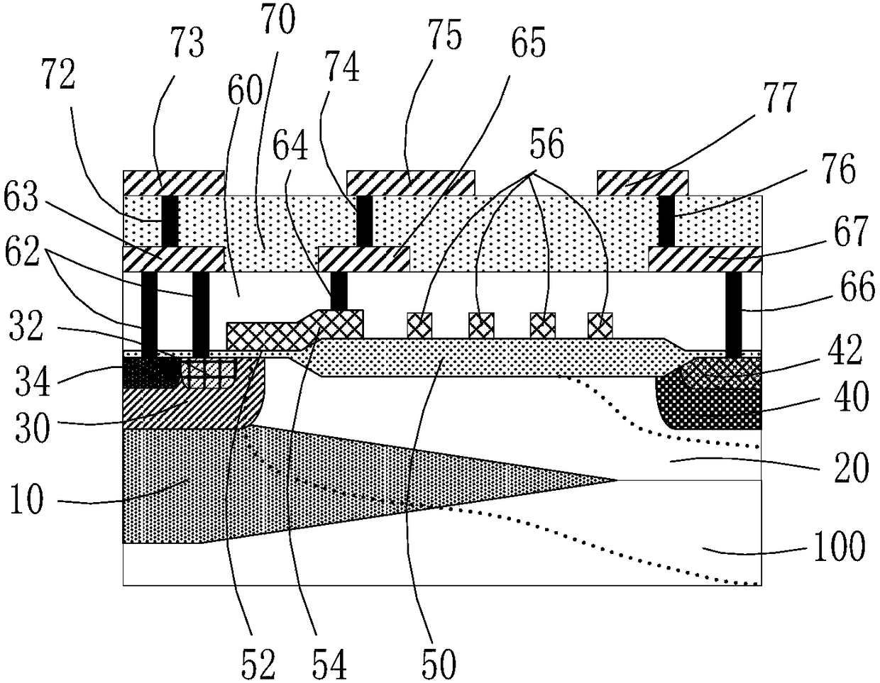
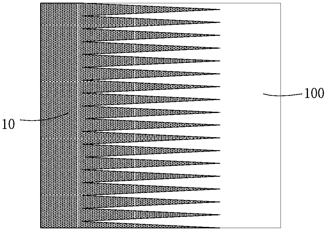
[0052]In describing the present invention, it should be understood that the terms "center", "longitudinal", "transverse", "upper", "lower", "front", "rear", "left", "right", " The orientations or positional relationships indicated by "vertical", "horizontal", "top", "bottom", "inner" and "outer" are based on the orientations or positional relationships shown in the drawings, and are only for the convenience of describing the present invention and Simplified descriptions, rather than indicating or implying that the device or element referred to must have a particular orientation, be constructed and operate in a particular orientation, and thus should not be construed as limiting the invention. In addition, the terms "first", "second", etc. are used for descriptive purposes only, and should not be understood a...


PUM

PropertyMeasurementUnit
Thicknessaaaaaaaaaa
Resistivityaaaaaaaaaa

Abstract

The present invention relates to a LDMOS (Lateral Double-diffused metal oxide semiconductor) and a manufacturing method thereof. A first buried layer with an impurity total amount gradually decreasedfrom left to right is injected and formed on a substrate, in the later diffusion process, the left side of the first buried layer is diffused towards the upper portion of an epitaxial layer due to theimpurities, the effective junction depth of the left side of the epitaxial layer becomes shallow, N-type impurities are decreased, when reverse bias is applied between the source and the drain of theLDMOS, the epitaxial layer region at the left side is easily exhausted, the exhaust line in the epitaxial layer region is rapidly extended towards the right with the increasing of the reversed bias voltage so as to have an effect on reduction of a peak electric field of the region, the junction depth of the region at right side of the first buried layer becomes shallow, P-type impurities are gradually decreased, the exhaust line of the P-type region can be rapidly extended towards a substrate region with a relative light concentration so as to rapidly reduce the electric field intensity of the drift region, improve the voltage endurance capability of the drift region and allow the device not to be untimely broken down in a vertical direction.

Description

technical field [0001] The invention belongs to the field of semiconductor manufacturing, and in particular relates to an LDMOS and a manufacturing method thereof. Background technique [0002] Lateral Double-diffused metal oxide semiconductor (LDMOS) is a high-voltage power device, which has the characteristics of high operating voltage, relatively simple process, and high switching frequency, and the processing technology based on bulk silicon materials is relatively mature. Therefore, LDMOS devices have broad development prospects. The drain, source and gate of the LDMOS device are all located on its surface, which is easy to integrate into the chip, so it is especially suitable as a high-voltage power device in high-voltage integrated circuits and power integrated circuits. [0003] In order to increase the breakdown voltage of LDMOS, a drift region is usually added between the source region and the drain region. When a reverse bias is applied between the source and dra...

Claims


Application Information

Patent Timeline
IPC IPC(8): H01L29/78H01L29/06H01L29/36H01L21/336
CPCH01L29/0684H01L29/36H01L29/66681H01L29/7816H01L29/0634H01L29/0692H01L29/0878H01L29/1083H01L29/1095H01L29/404H01L29/42368
Inventor 不公告发明人
Owner SHENZHEN NANSHUO MINGTAI TECH CO LTD
Why Eureka
Try Eureka