Graphite composite circuit board
A composite circuit and composite substrate technology, applied in circuit substrate materials, printed circuits, printed circuits, etc., can solve the problems of copper foil layer falling off, easy peeling, low peeling strength, etc. Effect
- Summary
- Abstract
- Description
- Claims
- Application Information
AI Technical Summary
Problems solved by technology
Method used
Image

Examples
Embodiment 1
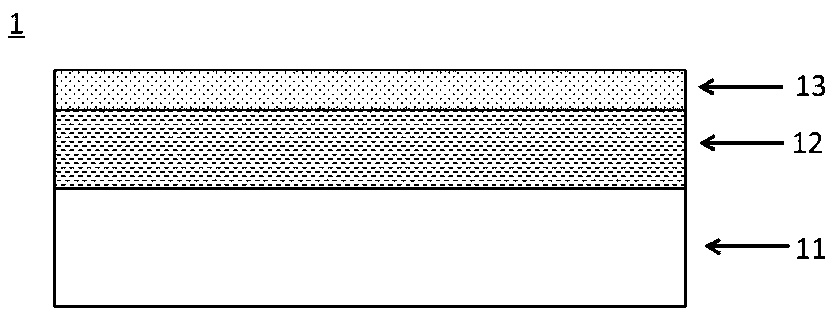
[0024] refer to figure 1 The graphite composite circuit board 1 comprises a substrate layer 11, a graphite composite layer 12 and a metal foil layer 13, and the graphite composite layer 12 bonds the substrate layer 11 and the metal foil layer 13 together.
[0025] According to different applications, the thickness of the substrate layer 11 is 10-9000 μm, and the material can be a metal substrate, a metal composite substrate, a ceramic substrate, a carbon substrate, a polymer substrate or a polymer composite substrate. in:
[0026] The metal substrate can be a pure metal plate or a metal alloy plate, such as aluminum plate, copper plate, aluminum alloy plate, copper alloy plate, titanium alloy plate, nickel alloy plate, stainless steel plate, etc.;
[0027] Metal composite substrates can be metal / ceramic composite boards, metal / diamond composite boards or metal / graphite composite boards, such as aluminum / ceramic powder composite boards, aluminum / diamond composite boards, alumi...
Embodiment 2
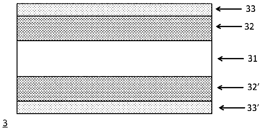
[0038] refer to image 3 , The graphite composite circuit board 3 comprises a substrate layer 31, two metal foil layers 33 and 33', and two graphite composite layers 32 and 32'. Metal foil layers 33, 33' are bonded to substrate layer 31 through graphite composite layers 32, 32' respectively. The substrate contains two metal foil layers and can be used as a two-layer circuit board.
[0039] In addition, the graphite composite circuit board of the present invention can be further expanded into a multilayer circuit board structure, such as Figure 4 As shown, the graphite composite circuit board 4 includes two substrate layers 411, 412, three metal foil layers 431, 432, 433, and graphite composite layers 421, 422, 423 or 424 are passed between adjacent substrate layers and metal foil layers. Bonded together to form a three-layer circuit board structure. Increase the number of substrate layers, metal foil layers and graphite composite layers, so that adjacent substrate layers a...
PUM
| Property | Measurement | Unit |
|---|---|---|
| Thickness | aaaaa | aaaaa |
| Size | aaaaa | aaaaa |
| Thickness | aaaaa | aaaaa |
Abstract
Description
Claims
Application Information
 - R&D
- Intellectual Property
- Life Sciences
- Materials
- Tech Scout
- Unparalleled Data Quality
- Higher Quality Content
- 60% Fewer Hallucinations
Browse by: Latest US Patents, China's latest patents, Technical Efficacy Thesaurus, Application Domain, Technology Topic, Popular Technical Reports.
© 2025 PatSnap. All rights reserved.Legal|Privacy policy|Modern Slavery Act Transparency Statement|Sitemap|About US| Contact US: help@patsnap.com