Laying method of monocrystal-like seed crystal

A laying method, single crystal-like technology, applied in the direction of single crystal growth, single crystal growth, chemical instruments and methods, etc., can solve the problems of poor compactness, inability to effectively recycle, reduce the proportion of high-efficiency single crystal silicon wafers, etc.

Inactive Publication Date: 2019-02-12
JINKO SOLAR CO LTD +1
View PDF4 Cites 2 Cited by
  • Summary
  • Abstract
  • Description
  • Claims
  • Application Information

AI Technical Summary

Problems solved by technology

[0003] However, there are following problems in the existing quasi-single crystal ingot casting process: such as figure 1 as shown, figure 1 It is a schematic diagram of laying the bottom of a single crystal seed silicon block in the existing quasi-single crystal ingot casting process. It can be seen that when laying the bottom of the single crystal seed silicon block 102 in the crucible 101, the silicon block is in close contact with the silicon block state, but there will be vibrations during transportation, and thermal expansion will occur during high temperature. These factors will cause splicing seams 103 to appear between single crystal seed silicon blocks 102. During high temperature melting, the silicon melt will As the splicing seam 103 flows downward, since the temperature of the lower part is lower than that of the upper part, the silicon melt flowing to the lower part will be cooled and solidified and seeded heterogeneously, resulting in polycrystalline formation in this region, and the resulting defects will be reduced. Proportion of high-efficiency monocrystalline silicon wafers
In view of the above problems, the main solution at present is to increase the area of ​​the seed crystal block to reduce the splicing area of ​​the seed crystal, or to lay a barrier layer of granular materials on the top of the seed crystal layer, but due to its relatively poor compactness, it is still due to splicing. Polycrystalline is produced due to joints, and the cost of single crystal seed crystal drawing is relatively high. There are many processes for making single crystal seed crystals into single crystal-like special seed crystal blocks, and it cannot be effectively recycled after ingot casting

Method used


Image

  • Laying method of monocrystal-like seed crystal
  • Laying method of monocrystal-like seed crystal
  • Laying method of monocrystal-like seed crystal

Examples


Embodiment Construction

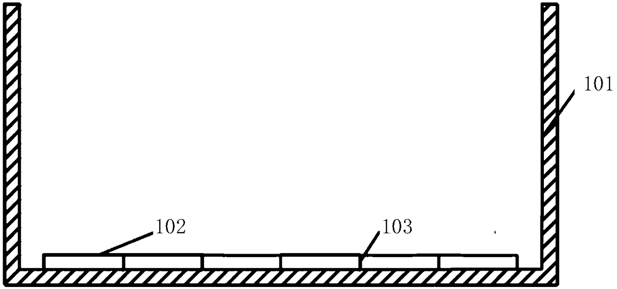
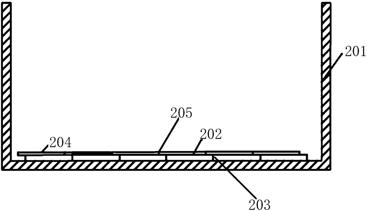
[0019] The core of the present invention is to provide a method for laying quasi-single crystal seed crystals, which can prevent the silicon melt from flowing down along the splicing seam and cooling and solidifying to produce polycrystals, thereby increasing the proportion of high-efficiency single crystal silicon wafers and reducing production costs.

[0020] The technical solutions in the embodiments of the present invention will be clearly and completely described below with reference to the accompanying drawings in the embodiments of the present invention. Obviously, the described embodiments are only a part of the embodiments of the present invention, but not all of the embodiments. Based on the embodiments of the present invention, all other embodiments obtained by those of ordinary skill in the art without creative efforts shall fall within the protection scope of the present invention.

[0021] An example of a method for laying single-crystal-like seed crystals provide...


PUM


Abstract

The invention discloses a laying method of monocrystal-like seed crystal which comprises the steps: tightly laying a first layer of monocrystal seed crystal with the thickness the same as the seed crystal melting finish leapfrog height at the bottom of a crucible; tightly laying a second layer of monocrystal seed crystal on the first layer of monocrystal seed crystal in a staggered mode, wherein joint seams of the second layer of monocrystal seed crystal and the joint seams of the first layer of monocrystal seed crystal are mutually staggered, so that even if joint seams are generated among the second layer of monocrystal seed crystal due to transportation or high temperature, high-temperature molten liquid penetrates through the joint seams among the second layer of monocrystal seed crystal but cannot enter the joint seams among the first layer of monocrystal seed crystal; namely, the laying method can prevent silicon melt from flowing downwards along the joint seams and being cooledand solidified to generate polycrystal; thus, the proportion of high-efficiency monocrystalline silicon pieces is improved, and the production cost is reduced.

Description

technical field [0001] The invention belongs to the technical field of photovoltaic equipment manufacturing, and particularly relates to a method for laying quasi-single crystal seed crystals. Background technique [0002] At present, the photovoltaic market has a high demand for high-efficiency and low-cost silicon wafers. Polycrystalline ingots have the advantage of low cost, but the efficiency improvement encounters technical bottlenecks. Monocrystalline has the advantage of high efficiency, but the drawing cost is high. In view of the above In this case, monocrystalline ingot-like technology has become a key development direction. [0003] However, there are the following problems in the existing single-crystal-like ingot casting process: such as figure 1 shown, figure 1 It is a schematic diagram of bottoming the single crystal seed crystal silicon block in the existing single crystal ingot-like ingot process. It can be seen that when the single crystal seed crystal si...

Claims


Application Information

Patent Timeline
IPC IPC(8): C30B11/14C30B28/06C30B29/06
Inventor 黄晶晶张涛肖贵云丁云飞梅坤姜志兴叶鹏金浩
Owner JINKO SOLAR CO LTD
Why Eureka
Try Eureka