A dual-wavelength semiconductor laser chip structure

A chip structure and semiconductor technology, applied in the direction of semiconductor laser device, laser device, active region structure, etc., can solve the problems of complex process, increase product cost, no cost advantage, etc., achieve simple manufacturing process and reduce manufacturing cost Effect

Active Publication Date: 2020-03-27
Shandong Huaguang Optoelectronics Co. Ltd.
View PDF8 Cites 0 Cited by
  • Summary
  • Abstract
  • Description
  • Claims
  • Application Information

AI Technical Summary

Problems solved by technology

The above two methods greatly increase the product cost and the process is complicated, especially in the application of small and medium power lasers, there is no cost advantage

Method used


Image

  • A dual-wavelength semiconductor laser chip structure

Examples


Embodiment 1

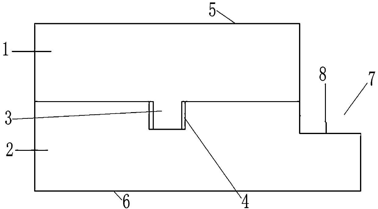
[0024] Further, it also includes a notch-shaped deep groove 7 arranged on the outer end of the epitaxial wafer II 2, the upper end surface of the epitaxial wafer I 1 is provided with a negative electrode I 5 conducting with the strip-shaped light emitting region 3, and the lower end surface of the epitaxial wafer II 2 is provided with There is a negative electrode II 6 connected to the groove-shaped light emitting region 4, and a positive electrode 8 connected to the strip-shaped light emitting region 3 and the groove-shaped light emitting region 4 is arranged on the upper end surface of the deep groove 7. By setting the deep groove 7 on the epitaxial wafer II 2, the strip-shaped light-emitting area 3 and the groove-shaped light-emitting area 4 can share a positive electrode 8, thereby further optimizing the structure and reducing the manufacturing cost.

Embodiment 2

[0026] Preferably, the width of the bar-shaped light-emitting region 3 of the dual-wavelength semiconductor laser chip structure is 4 . The width of the slot-shaped light-emitting area 4 is 8 .

Embodiment 3

[0028] Preferably, the width of the deep groove 7 of the dual-wavelength semiconductor laser chip structure is 200 , whose depth is 10-30 .


PUM


Abstract

A dual-wavelength semiconductor laser chip structure comprises an epitaxial wafer I and an epitaxial wafer II. The lower end face of the epitaxial wafer I is provided with an outwardly-protruding strip light-emitting area in width of 3-4micron; the upper end face of the epitaxial wafer II is provided with an inwardly-recessed grooved light-emitting area in width of 8-10micron. The lower end face of the epitaxial wafer I is fixedly adhered to the upper end face of the epitaxial wafer II, and the strip light-emitting area is inserted into the corresponding grooved light-emitting area. The epitaxial wafer I and the epitaxial wafer II are adhered through an adhesion process, and the strip light-emitting area of the epitaxial wafer I is inserted into the grooved light-emitting area of the epitaxial wafer II to form a laser chip with the characteristic of simultaneous emitting of dual-wavelength laser. A manufacturing process is simple, and the dual-wavelength semiconductor laser chip structure can be completely applied to fields of dual-wavelength laser medicine and night vision gun sight. Due to avoiding of a light coupling technique and complex optical lenses, manufacturing cost of dual-wavelength semiconductor lasers is sharply reduced.

Description

technical field [0001] The utility model relates to the field of semiconductor lasers, in particular to a dual-wavelength semiconductor laser chip structure. Background technique [0002] Semiconductor lasers have the advantages of high efficiency, long life, high beam quality, good stability, and compact structure. They are widely used in optical fiber communication, laser pumping, medical equipment, ordnance gun sights, laser printers and other fields. Since the birth of laser, laser technology has been an effective means of clinical treatment, and has gradually developed into a key technology of medical diagnosis. It has solved many difficult problems in medicine and made contributions to the development of medicine. At present, laser medical treatment has formed a mature and stable market, and has maintained a strong momentum of development in its basic research, new technology development, new equipment development and production and other aspects. For more than 20 yea...

Claims


Application Information

Patent Timeline
Patent Type & Authority Patents(China)
IPC IPC(8): H01S5/30H01S5/40
CPCH01S5/30H01S5/40
Inventor 苏建李沛旭汤庆敏夏伟肖成峰
Owner Shandong Huaguang Optoelectronics Co. Ltd.
Why Eureka
Try Eureka