Manufacturing method of gallium nitride HEMT
A manufacturing method and gallium nitride technology, applied in the field of manufacturing, can solve the problems of interface distortion, defects, leakage withstand voltage, etc., and achieve the effects of stabilizing current-voltage characteristics, improving I-V characteristics, and improving ON withstand voltage.
- Summary
- Abstract
- Description
- Claims
- Application Information
AI Technical Summary
Problems solved by technology
Method used
Image

Examples
Embodiment Construction
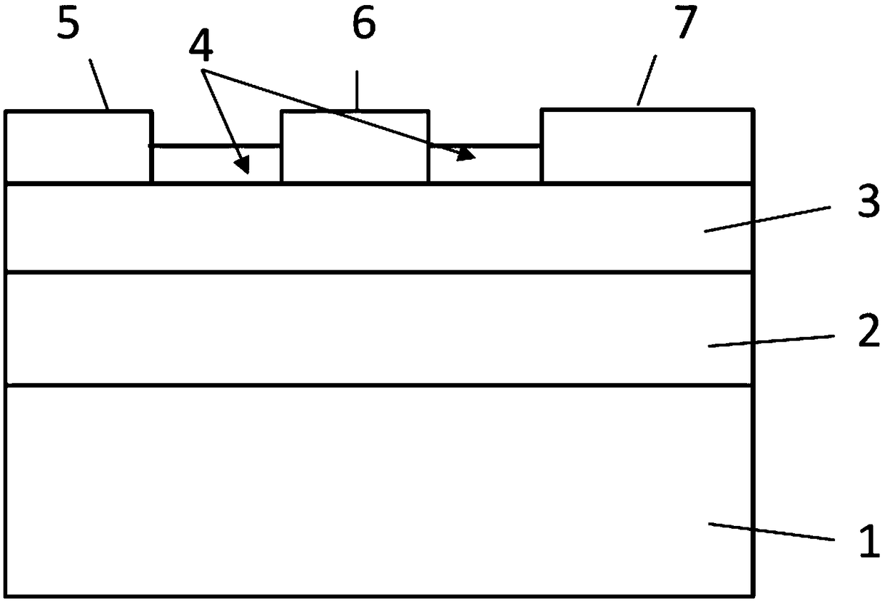
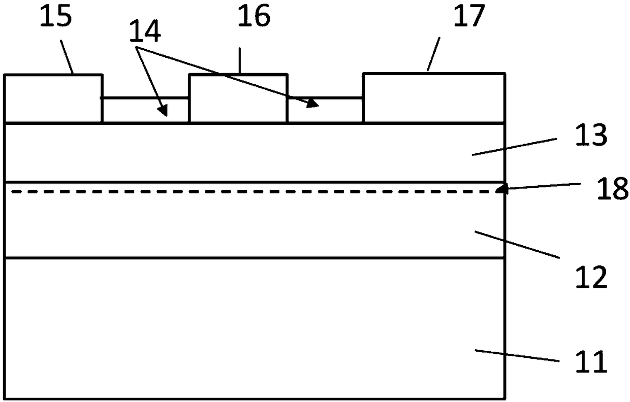
[0023] figure 1 The principle constitution of the invention is shown. Refer below figure 1 Means for solving the problems in the present invention will be described.
[0024] In the present invention, a GaN substrate 1 is prepared first, a GaN electron moving layer 2 is constructed on the GaN substrate 1, and an AlxGa1-xN (0
[0025] In this way, the three electrodes on the electron supply layer 3 are sequentially arranged in the order of the source 5, the drain 6, and the gate 7, the piezoelectric charge raises the energy band, and the tunnel current decreases, thereby improving the Schottky characteristic. . The voids generated near the interface cancel each other out, and because the influence of surface traps caused by aluminum (Al) can be eliminated, stable IV...
PUM
 Abstract
Description
Claims
Application Information
 - R&D
- Intellectual Property
- Life Sciences
- Materials
- Tech Scout
- Unparalleled Data Quality
- Higher Quality Content
- 60% Fewer Hallucinations
Browse by: Latest US Patents, China's latest patents, Technical Efficacy Thesaurus, Application Domain, Technology Topic, Popular Technical Reports.
© 2025 PatSnap. All rights reserved.Legal|Privacy policy|Modern Slavery Act Transparency Statement|Sitemap|About US| Contact US: help@patsnap.com